| ID |
Date |
Author |
Subject |
|
597
|
Tue Apr 23 13:15:43 2024 |
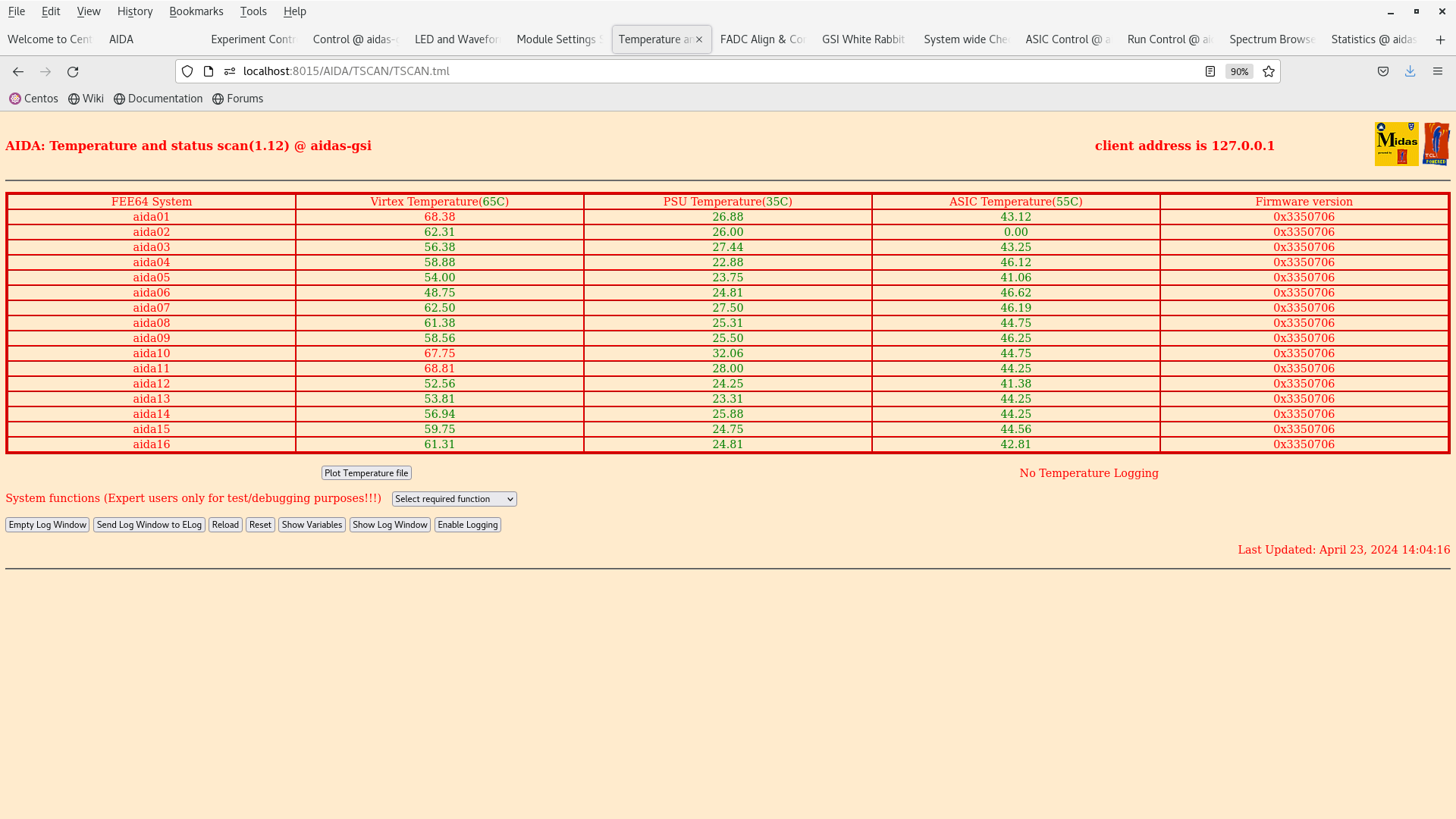
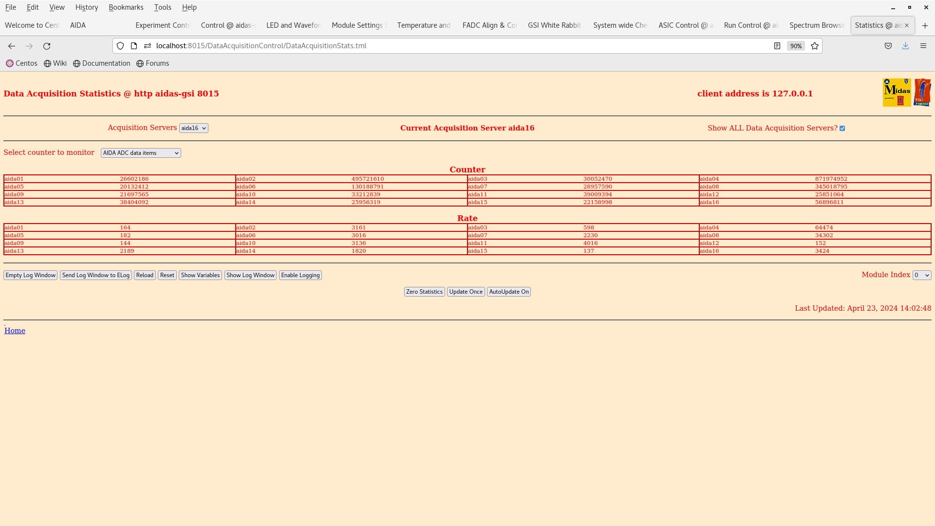
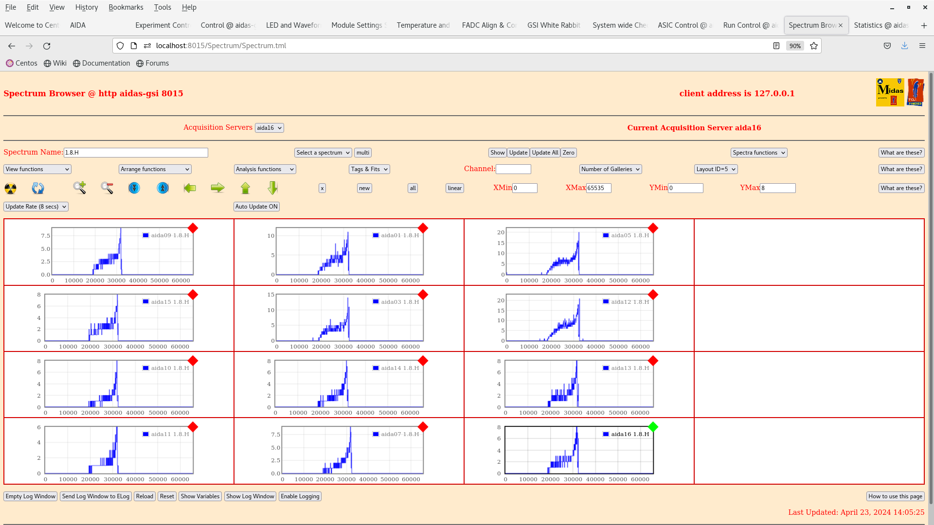
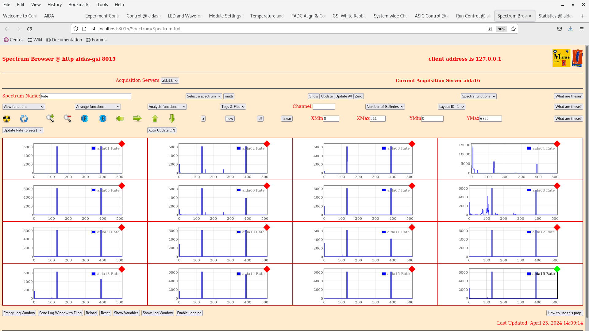
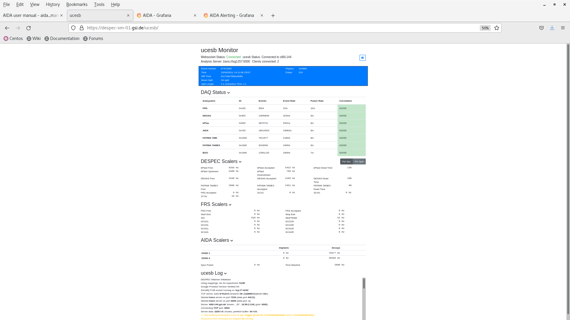
PP | 14:00 checks |
All looks good.
Screenshots attached |
| Attachment 1: Screenshot_from_2024-04-23_14-11-33.png
|

|
| Attachment 2: Screenshot_from_2024-04-23_14-04-26.png
|
|
| Attachment 3: Screenshot_from_2024-04-23_14-04-44.png
|
|
| Attachment 4: Screenshot_from_2024-04-23_14-06-02.png
|
|
| Attachment 5: Screenshot_from_2024-04-23_14-07-07.png
|

|
| Attachment 6: Screenshot_from_2024-04-23_14-09-26.png
|
|
| Attachment 7: Screenshot_from_2024-04-23_14-10-55.png
|

|
| Attachment 8: Screenshot_from_2024-04-23_14-11-16.png
|
|
|
599
|
Tue Apr 23 19:23:42 2024 |
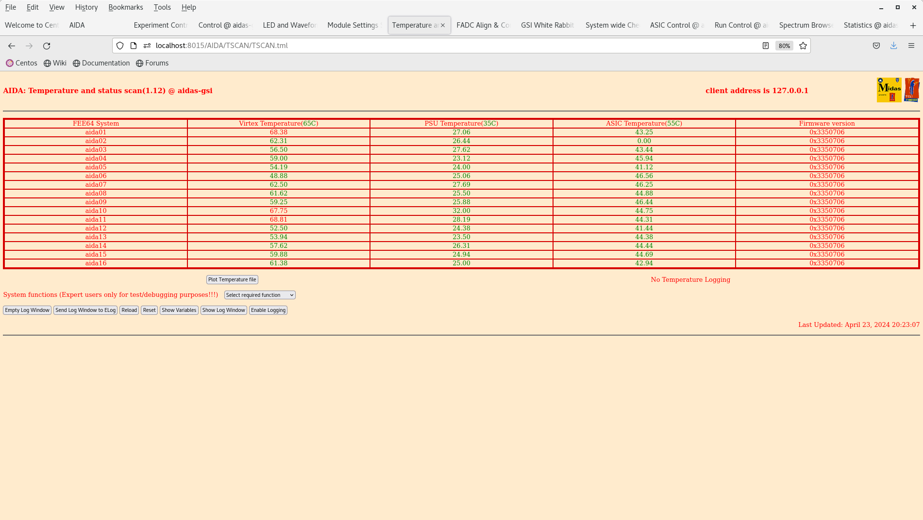
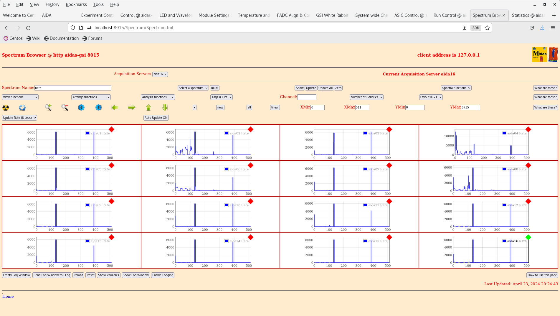
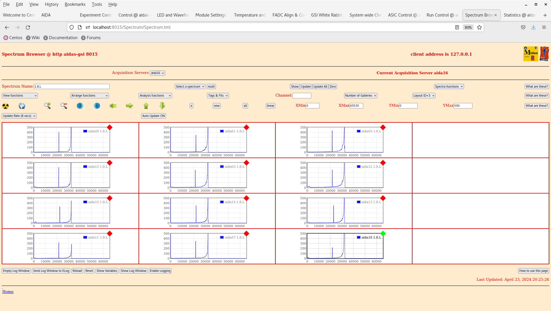
PP | 20:30 checks |
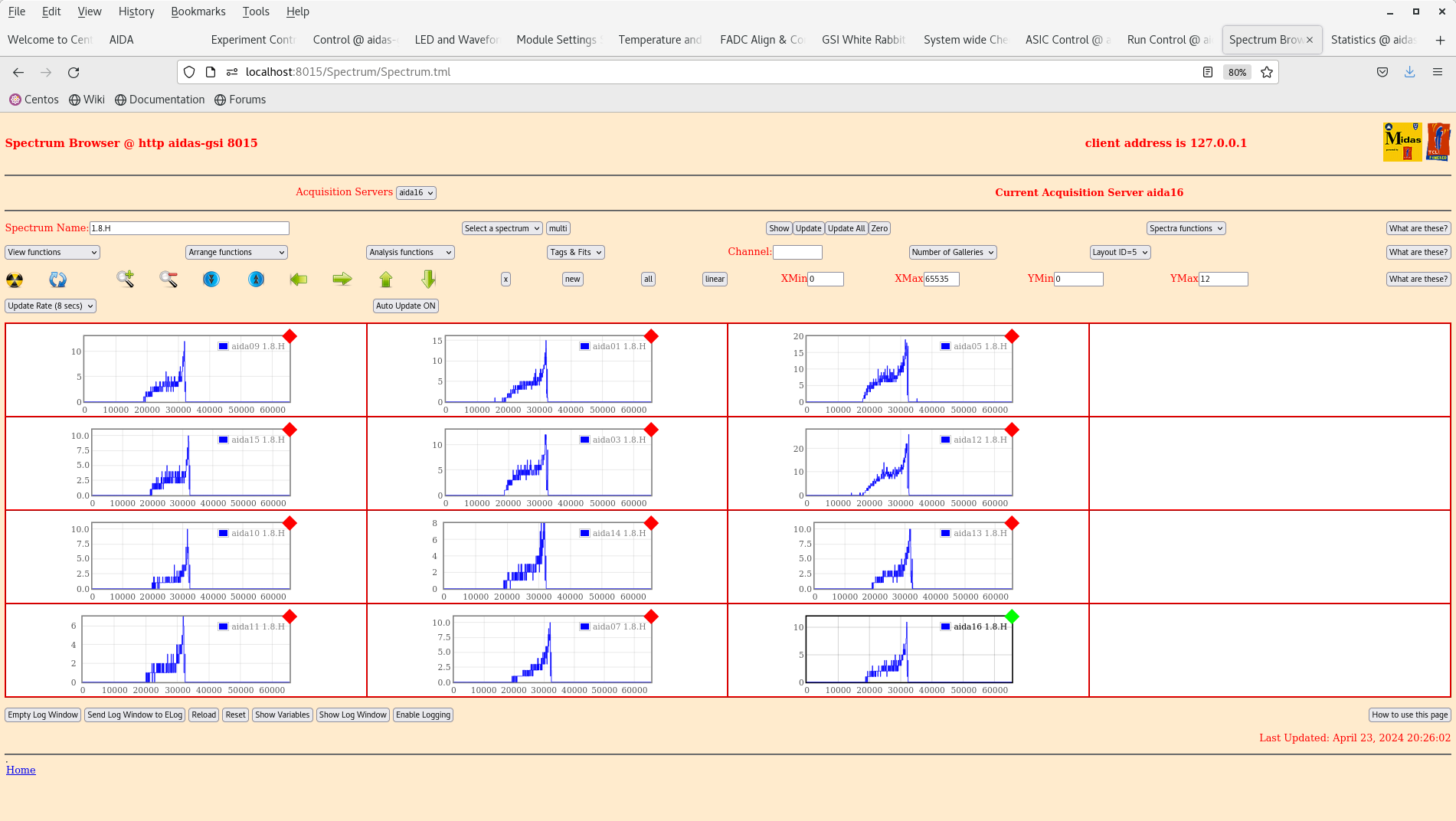
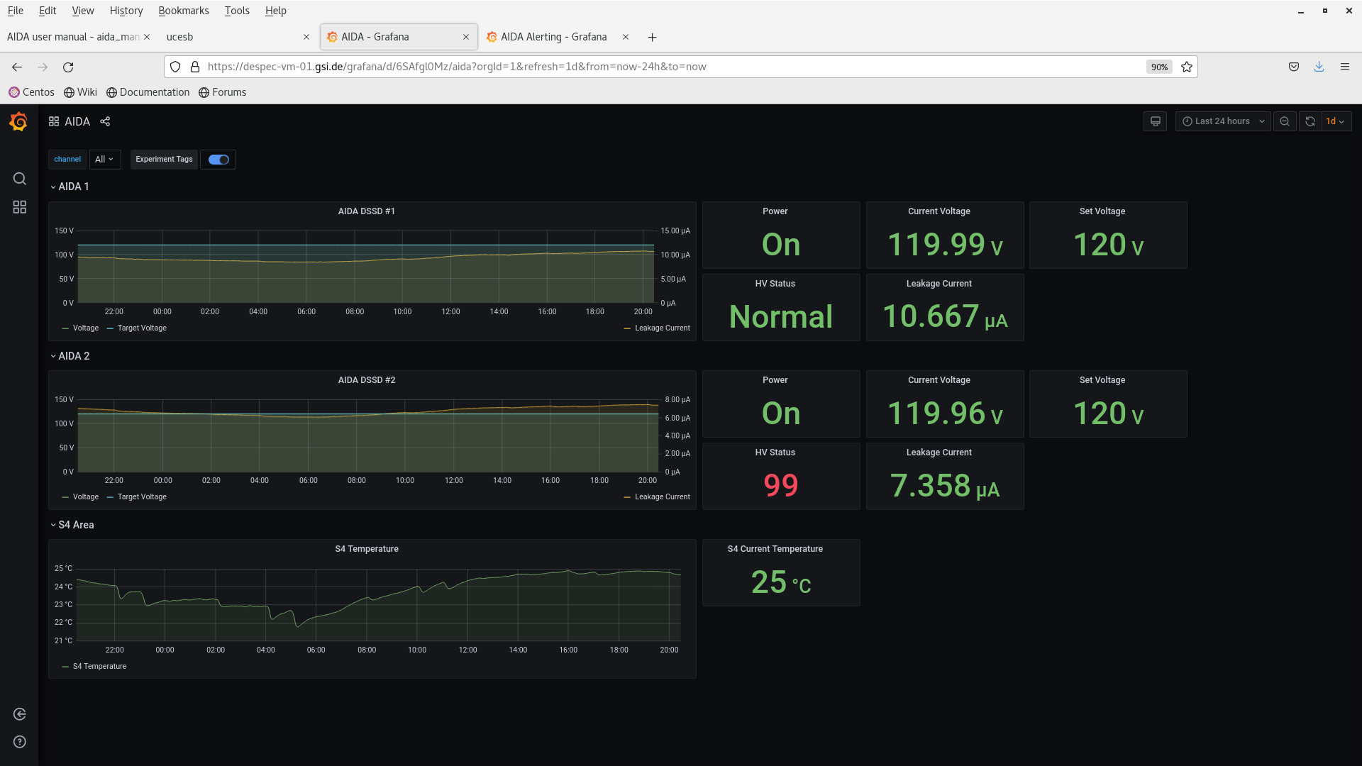
All looks good.
Screenshots attached. |
| Attachment 1: Screenshot_from_2024-04-23_20-24-09.png
|
|
| Attachment 2: Screenshot_from_2024-04-23_20-24-25.png
|

|
| Attachment 3: Screenshot_from_2024-04-23_20-24-52.png
|
|
| Attachment 4: Screenshot_from_2024-04-23_20-25-35.png
|
|
| Attachment 5: Screenshot_from_2024-04-23_20-26-16.png
|
|
| Attachment 6: Screenshot_from_2024-04-23_20-27-01.png
|

|
| Attachment 7: Screenshot_from_2024-04-23_20-27-26.png
|
|
| Attachment 8: Screenshot_from_2024-04-23_20-27-53.png
|

|
|
602
|
Wed Apr 24 15:37:59 2024 |
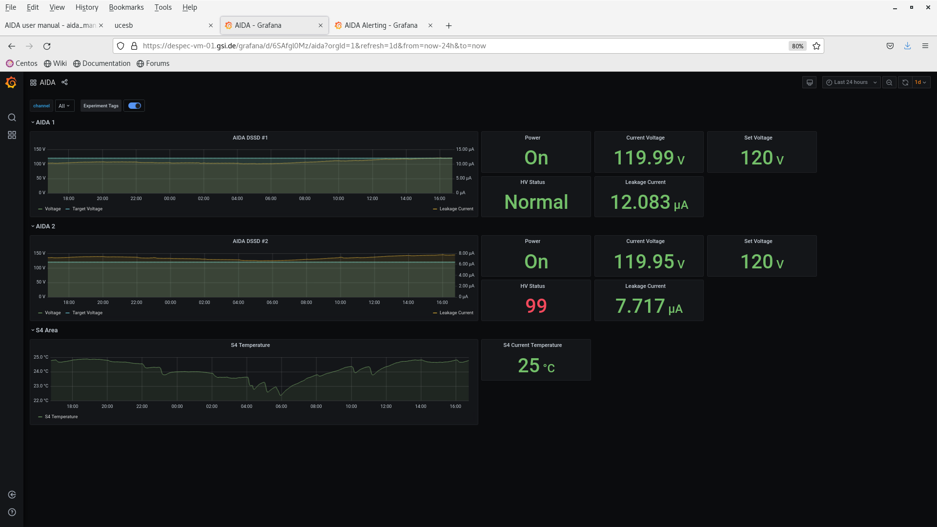
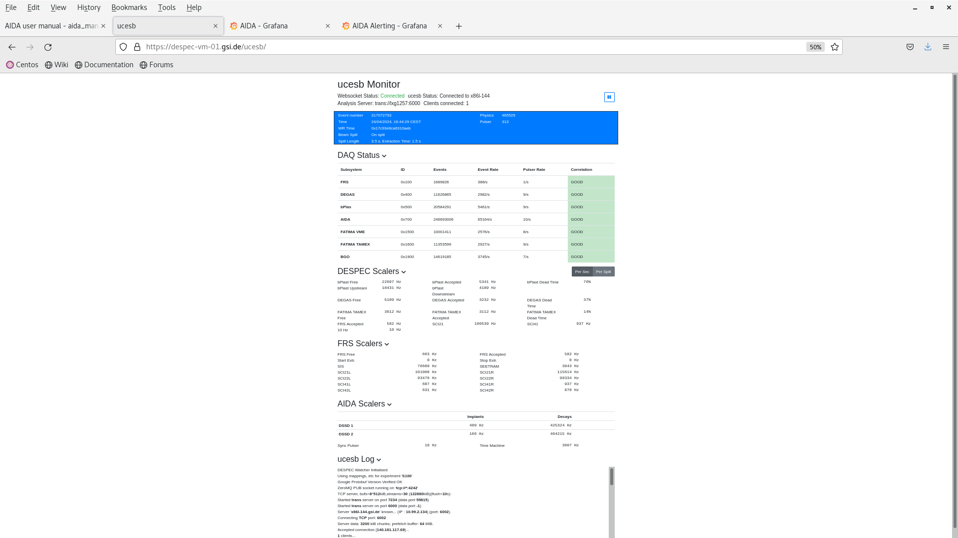
PP | 16:00-00:00 shift Wednesday 24 April |
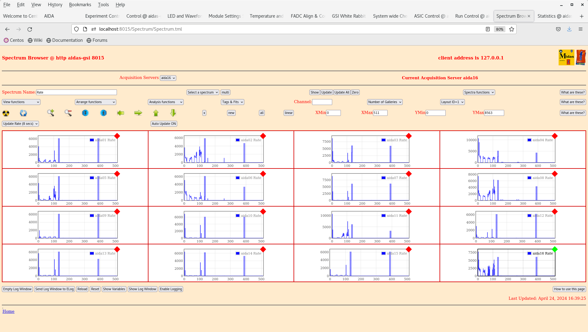
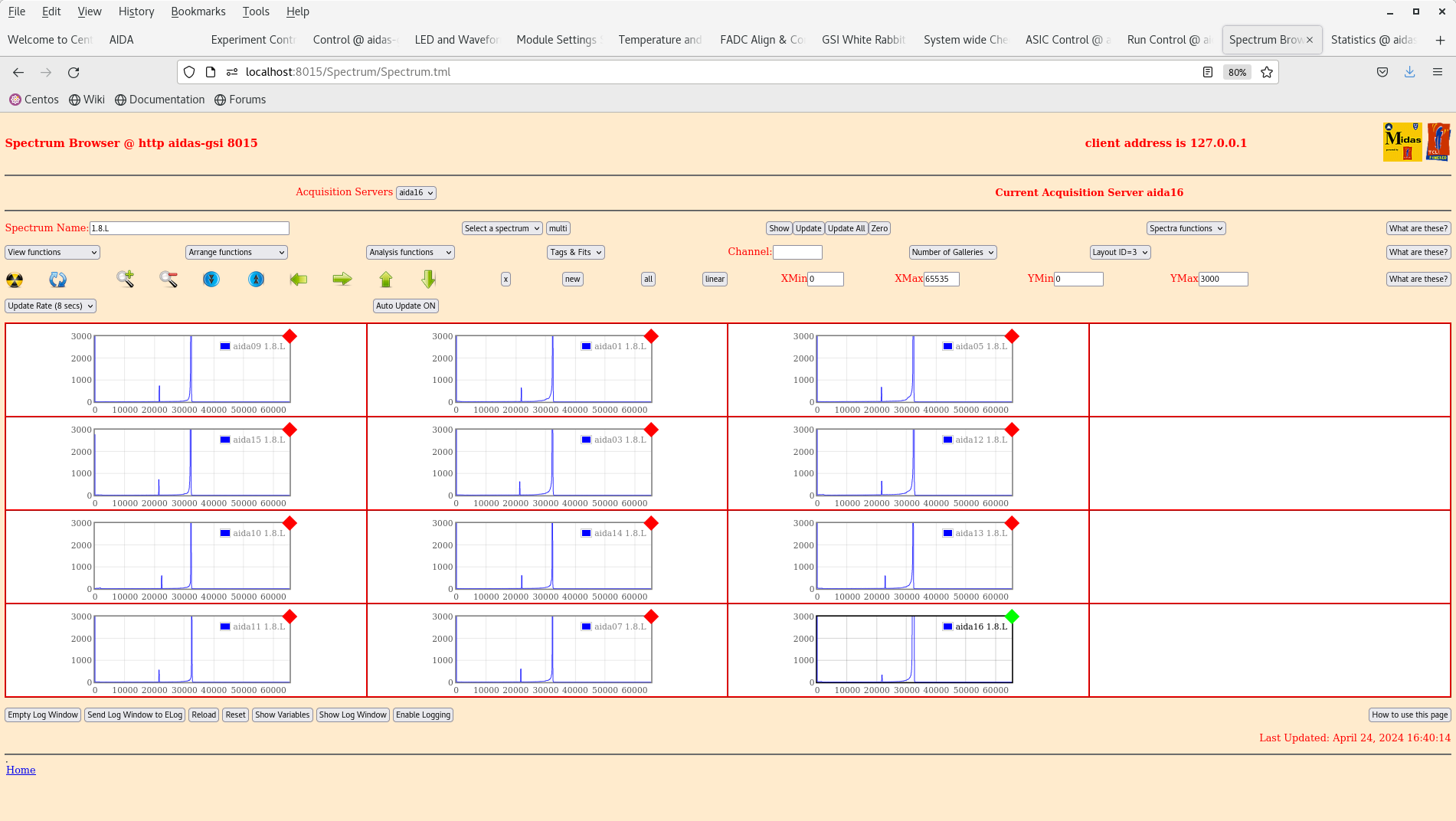
All seems OK.
Screenshots attached. |
| Attachment 1: Screenshot_from_2024-04-24_16-38-45.png
|

|
| Attachment 2: Screenshot_from_2024-04-24_16-39-09.png
|

|
| Attachment 3: Screenshot_from_2024-04-24_16-39-38.png
|
|
| Attachment 4: Screenshot_from_2024-04-24_16-40-24.png
|
|
| Attachment 5: Screenshot_from_2024-04-24_16-41-15.png
|

|
| Attachment 6: Screenshot_from_2024-04-24_16-43-41.png
|

|
| Attachment 7: Screenshot_from_2024-04-24_16-44-15.png
|
|
| Attachment 8: Screenshot_from_2024-04-24_16-44-32.png
|
|
|
603
|
Wed Apr 24 18:44:05 2024 |
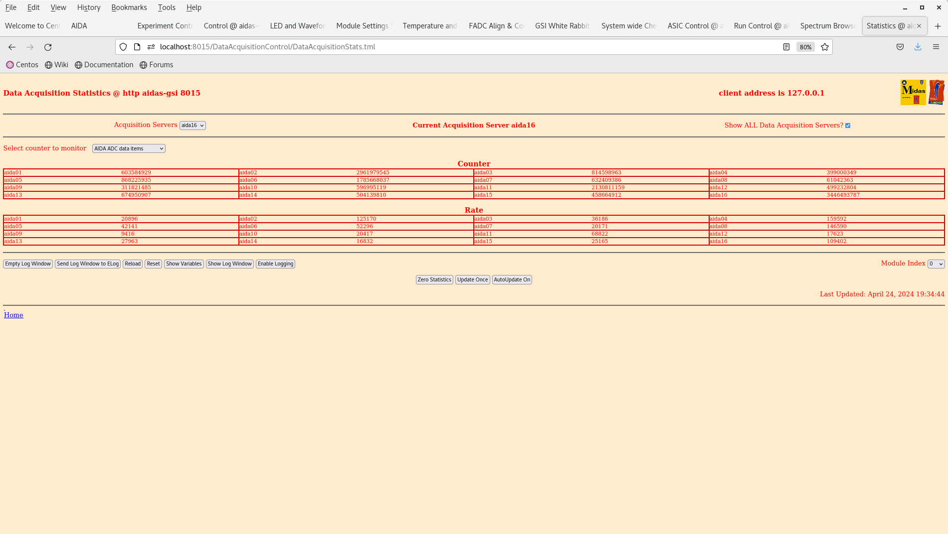
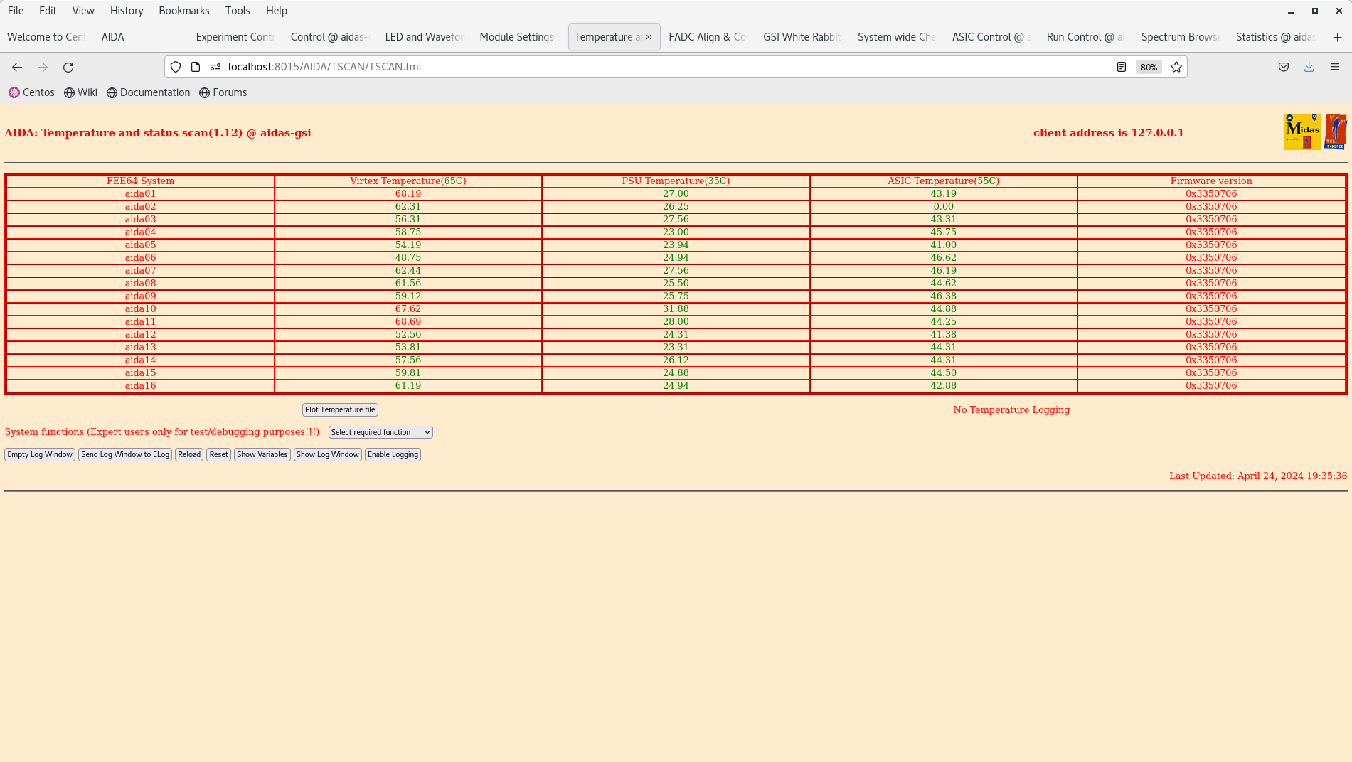
PP | 19:30 checks |
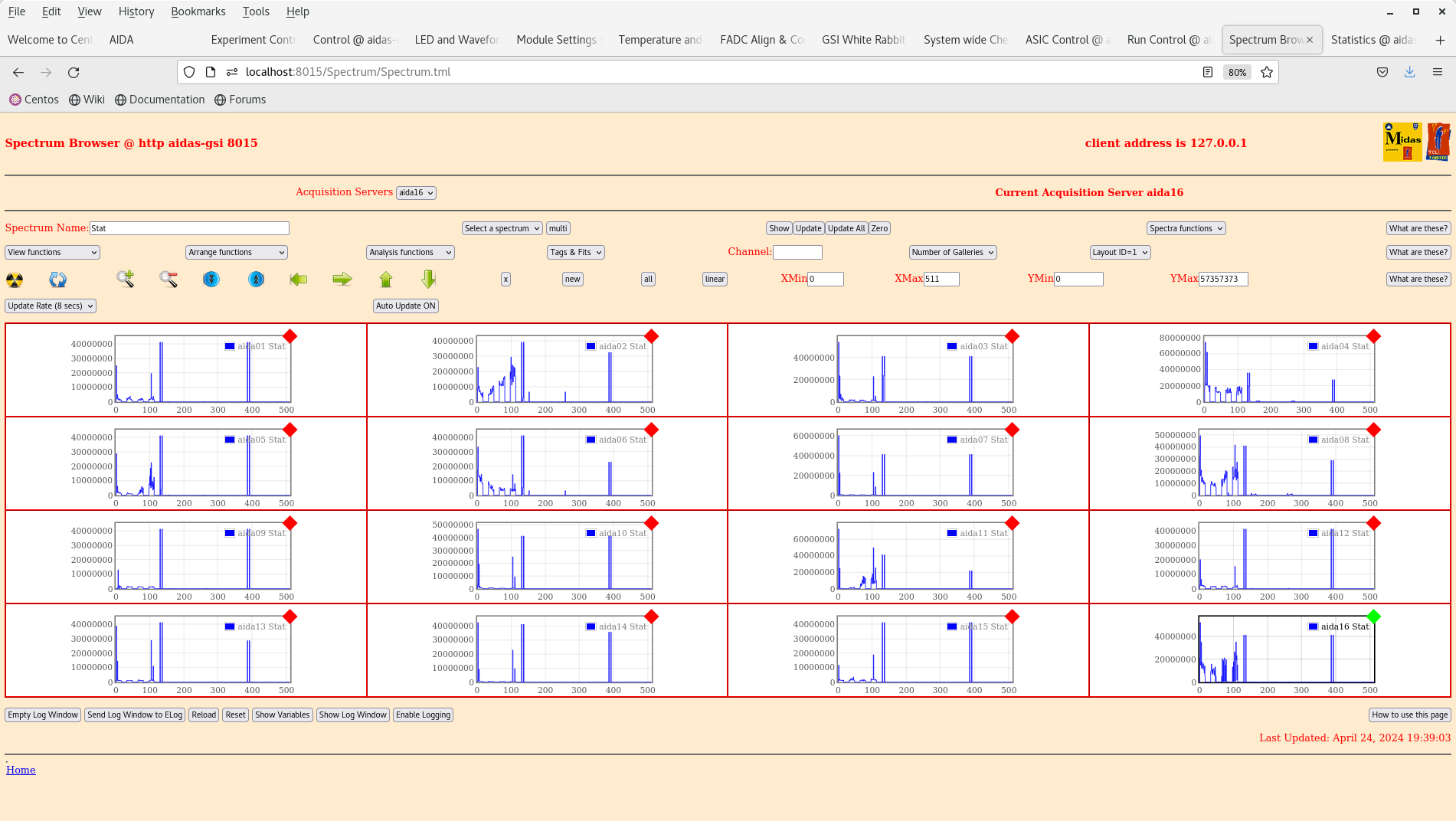
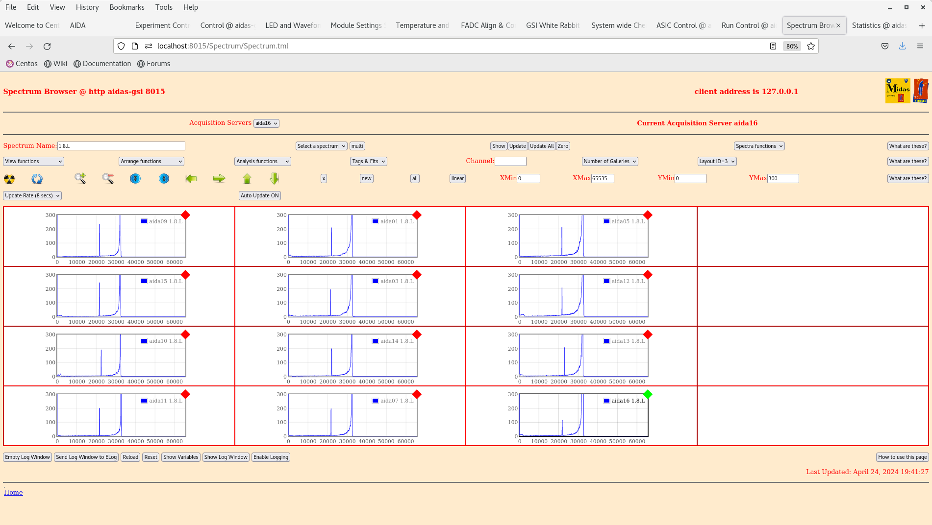
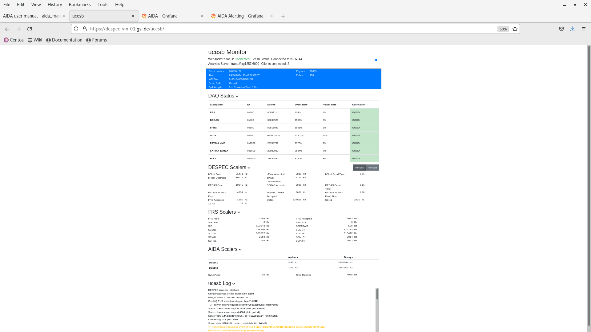
All seems smooth.
Screenshots attached. |
| Attachment 1: Screenshot_from_2024-04-24_19-34-58.png
|
|
| Attachment 2: Screenshot_from_2024-04-24_19-37-12.png
|
|
| Attachment 3: Screenshot_from_2024-04-24_19-40-36.png
|
|
| Attachment 4: Screenshot_from_2024-04-24_19-41-39.png
|
|
| Attachment 5: Screenshot_from_2024-04-24_19-42-20.png
|

|
| Attachment 6: Screenshot_from_2024-04-24_19-42-53.png
|

|
| Attachment 7: Screenshot_from_2024-04-24_19-43-21.png
|

|
| Attachment 8: Screenshot_from_2024-04-24_19-43-41.png
|
|
|
652
|
Tue Jun 11 18:45:37 2024 |
PP | Mid-shift checks, 19:45 |
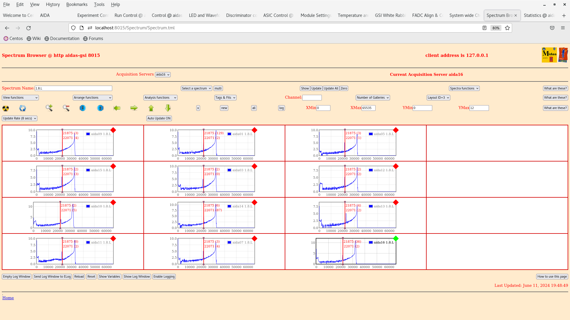
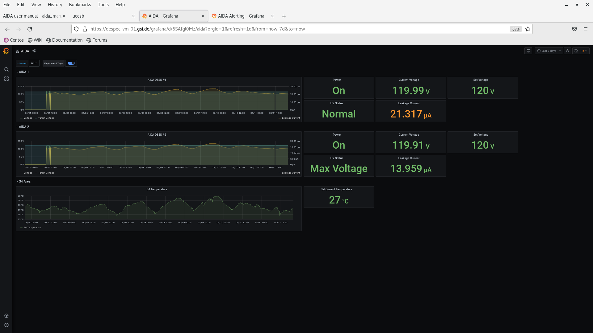
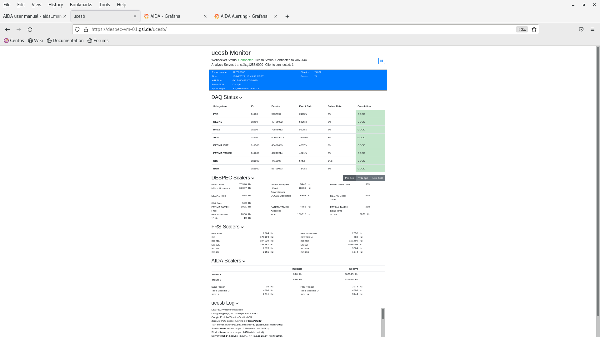
All looks good.
Sceenshots attached. |
| Attachment 1: Screenshot_from_2024-06-11_19-46-41.png
|

|
| Attachment 2: Screenshot_from_2024-06-11_19-47-09.png
|

|
| Attachment 3: Screenshot_from_2024-06-11_19-47-38.png
|

|
| Attachment 4: Screenshot_from_2024-06-11_19-48-12.png
|

|
| Attachment 5: Screenshot_from_2024-06-11_19-48-58.png
|
|
| Attachment 6: Screenshot_from_2024-06-11_19-49-22.png
|
|
| Attachment 7: Screenshot_from_2024-06-11_19-49-43.png
|
|
| Attachment 8: Screenshot_from_2024-06-11_19-50-19.png
|

|
|
656
|
Wed Jun 12 11:06:55 2024 |
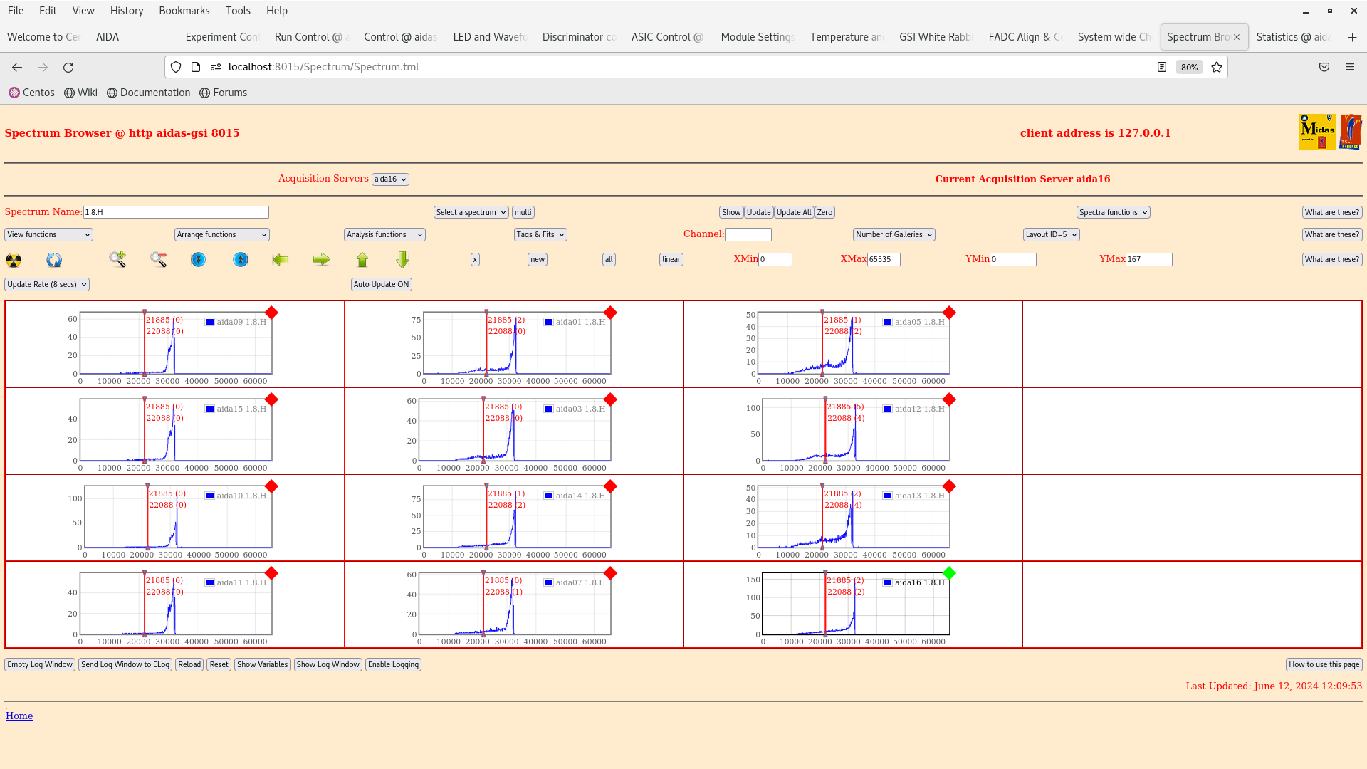
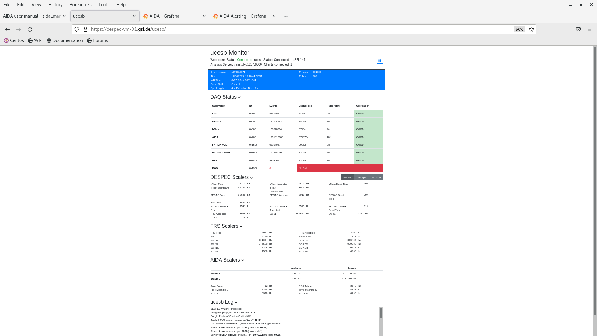
PP | Mid-shift checks, 12:00 |
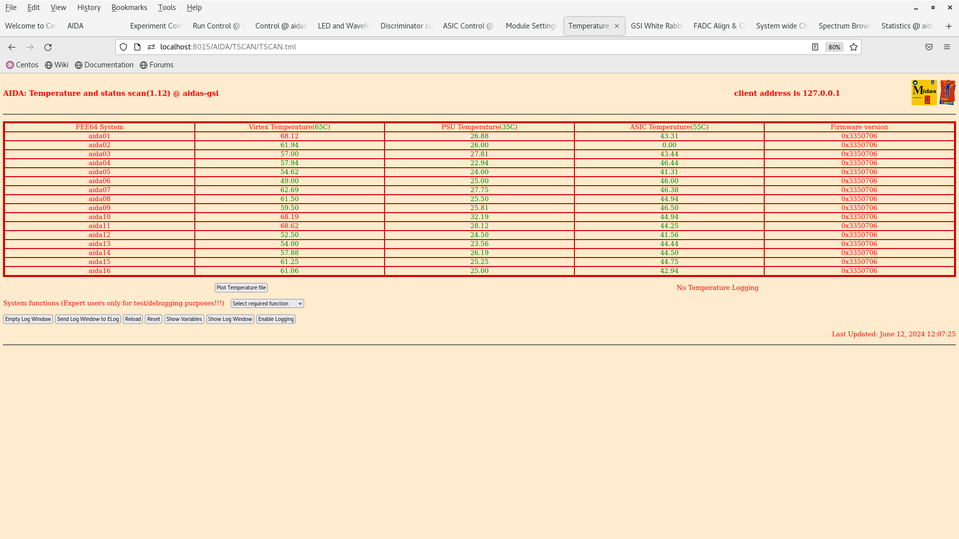
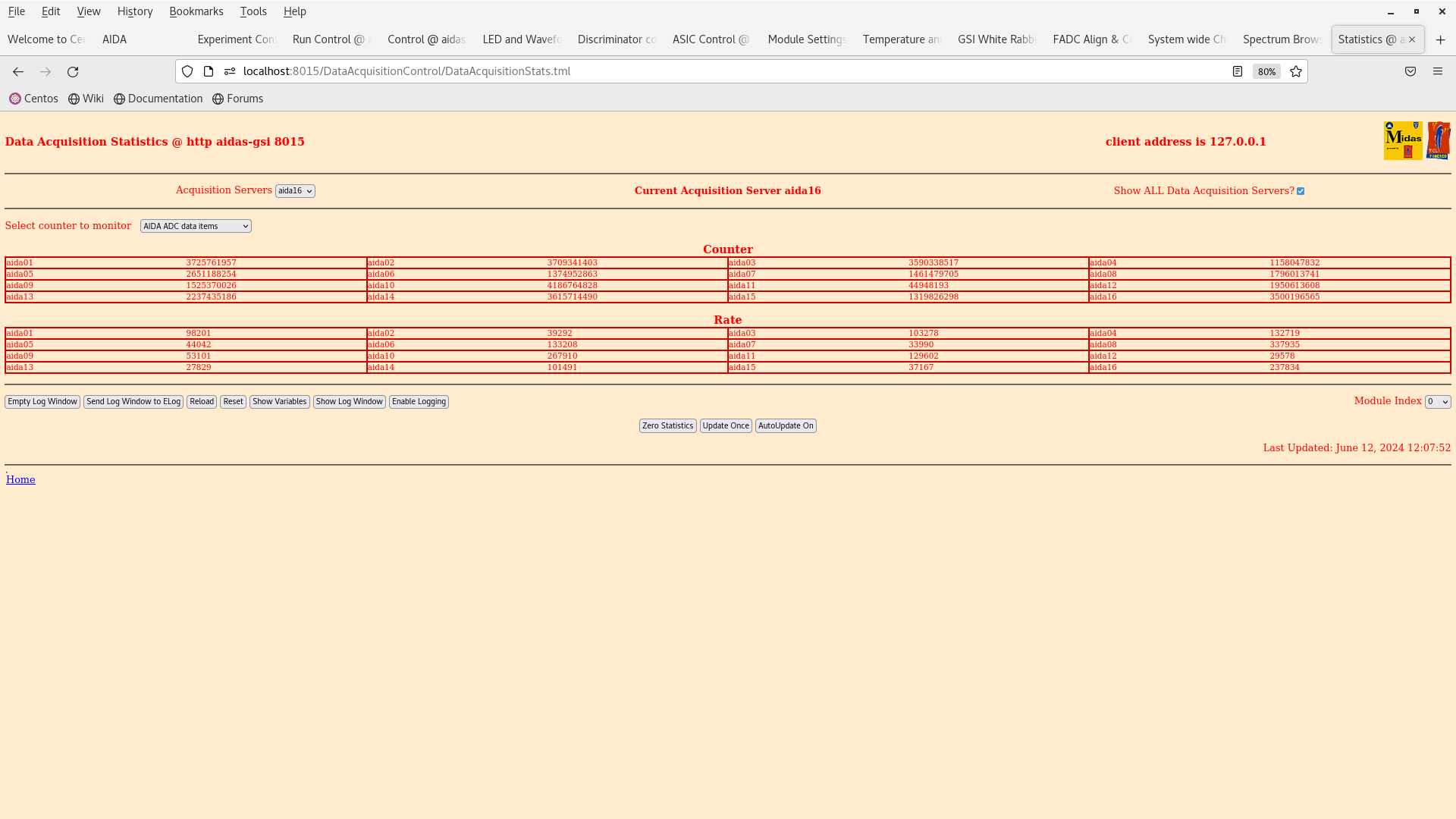
All seems normal.
Screenshots attached. |
| Attachment 1: Screenshot_from_2024-06-12_12-07-32.png
|
|
| Attachment 2: Screenshot_from_2024-06-12_12-07-59.png
|
|
| Attachment 3: Screenshot_from_2024-06-12_12-08-24.png
|

|
| Attachment 4: Screenshot_from_2024-06-12_12-09-09.png
|

|
| Attachment 5: Screenshot_from_2024-06-12_12-10-02.png
|
|
| Attachment 6: Screenshot_from_2024-06-12_12-10-30.png
|

|
| Attachment 7: Screenshot_from_2024-06-12_12-10-46.png
|
|
| Attachment 8: Screenshot_from_2024-06-12_12-11-41.png
|

|
|
517
|
Wed Jan 18 13:40:33 2023 |
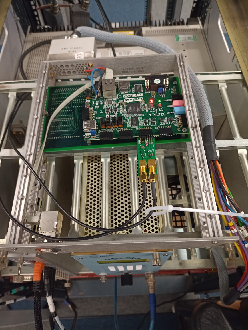
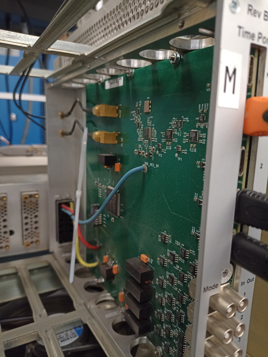
PJCS TD | MACB settings with either Emulator or VITAR |
When using the VETAR connected to the HDMI port of the root MACB the settings for all the MACB in the system 0x3.
This setting takes the Clock and Data line from the input HDMI and outputs it via teh HDMI output ports.
When using the Emulator connected via the SMA connectors on the back of the root MACB then the setting for the root MACB should be 0xD and all others should be 0x3.
Attached is the .jed file for programming the MACB and the .vhd source file to help with understanding of the settings. |
| Attachment 1: macb_apr20.jed
|
| Attachment 2: macb_apr20.vhd
|
----------------------------------------------------------------------------------
-- Company:
-- Engineer:
--
-- Create Date:    17:03:27 03/16/2011
-- Design Name:
-- Module Name:    macb_top - Behavioral
-- Project Name:
-- Target Devices:
-- Tool versions:
-- Description:
--
-- Dependencies:
--
-- Revision:
-- Revision 0.01 - File Created
-- Additional Comments:
--
----------------------------------------------------------------------------------
library IEEE;
use IEEE.STD_LOGIC_1164.ALL;
use IEEE.STD_LOGIC_ARITH.ALL;
use IEEE.STD_LOGIC_UNSIGNED.ALL;

---- Uncomment the following library declaration if instantiating
---- any Xilinx primitives in this code.
library UNISIM;
use UNISIM.VComponents.all;
-- NOTE all in/out notations are relative to this unit
entity macb_apr20 is
    Port (
			  port1_sp : inout  STD_LOGIC_VECTOR (3 downto 0);
			  port2_sp : inout  STD_LOGIC_VECTOR (3 downto 0);
			  port3_sp : inout  STD_LOGIC_VECTOR (3 downto 0);
			  port4_sp : inout  STD_LOGIC_VECTOR (3 downto 0);
			  layer_sp : inout  STD_LOGIC_VECTOR (3 downto 0);
			  layer_trigger : out std_logic ;
           sync_return : in  STD_LOGIC_VECTOR (3 downto 1);
           selector : in  STD_LOGIC_VECTOR (3 downto 0);
           sync_select : out  STD_LOGIC_vector(1 downto 0 );
           clock200_select : out  STD_LOGIC_vector( 1 downto 0 ) ;
			  butis_divide_reset : out std_logic ;
			  butis_divide_s : out std_logic_vector( 2 downto 0 ) ;
			  clock_5 : in std_logic ;
			  sync_5 : in std_logic ;
			  trigger : in std_logic_vector( 3 downto 0 ) ;
           MBS_in : in  STD_LOGIC_VECTOR (3 downto 0);
           MBS_out : out  STD_LOGIC_VECTOR (3 downto 0));
end macb_apr20;

architecture Behavioral of macb_apr20 is
signal port1_spi :  STD_LOGIC_VECTOR (3 downto 0) := ( others => '0' );
signal port1_spo :  STD_LOGIC_VECTOR (3 downto 0) := ( others => '0' );
signal port1_t :  STD_LOGIC_VECTOR (3 downto 0) := ( others => '1' );
signal port2_spi :  STD_LOGIC_VECTOR (3 downto 0) := ( others => '0' );
signal port2_spo :  STD_LOGIC_VECTOR (3 downto 0) := ( others => '0' );
signal port2_t :  STD_LOGIC_VECTOR (3 downto 0) := ( others => '1' );
signal port3_spi :  STD_LOGIC_VECTOR (3 downto 0) := ( others => '0' );
signal port3_spo :  STD_LOGIC_VECTOR (3 downto 0) := ( others => '0' );
signal port3_t :  STD_LOGIC_VECTOR (3 downto 0) := ( others => '1' );
signal port4_spi :  STD_LOGIC_VECTOR (3 downto 0) := ( others => '0' );
signal port4_spo :  STD_LOGIC_VECTOR (3 downto 0) := ( others => '0' );
signal port4_t :  STD_LOGIC_VECTOR (3 downto 0) := ( others => '1' );
signal layer_spi :  STD_LOGIC_VECTOR (3 downto 0) := ( others => '0' );
signal layer_spo :  STD_LOGIC_VECTOR (3 downto 0) := ( others => '0' );
signal layer_t :  STD_LOGIC_VECTOR (3 downto 0) := ( others => '1' );
signal seli : integer range 0 to 15 := 0  ;
-- well really
signal MBS_in_n : std_logic_vector( 3 downto 0 ) := "0000" ;
begin
MBS_in_n <= ( not MBS_in);
seli <= conv_integer(not selector) ;
-- MBS signal allocations to sp lines and HDMI pin. This maps to NIM connections
-- 0 :	MBS_clock10 	SP0	13
-- 1 :	MBS_reset		SP1	14
-- 2 :	MBS_reset_rq	SP2	15
-- 3 :	MBS_Trigger		SP3	16
layer_trigger <= trigger(0) or trigger(1) or trigger(2) or trigger(3) ;

-- divider controls set for pass-through
butis_divide_reset <= '1' ; -- for now don't reset ;

process ( seli , MBS_in_n, port1_spi, port2_spi, port3_spi, port4_spi, layer_spi, sync_return ,sync_5  )
-- note : & => concatenate
begin
	case seli is
	when 0 => --- Master/ Root / MBS / Internal clock
		port1_spo <= MBS_in_n(3) & MBS_in_n(2) & '0' & '0' ;
		port1_t <= "0011" ; -- drive trigger and reset request only
		port2_spo <= MBS_in_n(3) & '0' & port1_spi(1) & port1_spi(0) ;
		port2_t <= "0100" ; -- drive clock, reset, trigger only
		port3_spo <= MBS_in_n(3) & '0' & port1_spi(1) & port1_spi(0) ;
		port3_t <= "0100" ; -- drive clock, reset, trigger only
		port4_spo <= MBS_in_n(3) & '0' & port1_spi(1) & port1_spi(0) ;
		port4_t <= "0100" ; -- drive clock, reset, trigger only
		layer_spo <= ( others => '0' ) ;
		layer_t <= ( others => '1' ) ; -- disable the drive to the "next" port
		sync_select <= "00" ; -- select sync from port 1
		clock200_select <= "00" ; -- select internal 200 MHz oscillator
		MBS_out <=  MBS_in_n(3) & MBS_in_n(2) & port1_spi(1) & port1_spi(0) ;
		butis_divide_s <= "000" ; -- s2 is 0 for pass,

	when 1 => --- Master/ Root / MBS / BuTiS clock and SYNC
		port1_spo <= MBS_in_n(3) & MBS_in_n(2) & '0' & '0' ;
		port1_t <= "0011" ; -- drive trigger and reset request only
		port2_spo <= MBS_in_n(3) & '0' & port1_spi(1) & port1_spi(0) ;
		port2_t <= "0100" ; -- drive clock, reset, trigger only
		port3_spo <= MBS_in_n(3) & '0' & port1_spi(1) & port1_spi(0) ;
		port3_t <= "0100" ; -- drive clock, reset, trigger only
		port4_spo <= MBS_in_n(3) & '0' & port1_spi(1) & port1_spi(0) ;
		port4_t <= "0100" ; -- drive clock, reset, trigger only
		layer_spo <= ( others => '0' ) ;
		layer_t <= ( others => '1' ) ; -- disable the drive to the "next" port
		sync_select <= "01" ; -- select sync from external using SMA input
		clock200_select <= "01" ; -- select external 200 MHz oscillator using SMA input
		MBS_out <=  MBS_in_n(3) & MBS_in_n(2) & port1_spi(1) & port1_spi(0) ;
		butis_divide_s <= "000" ; -- s2 is 0 for pass,

	when 2 => --- Master/ Branch / MBS / Next layer clock next layer SYNC
		port1_spo <= layer_spi(3) & layer_spi(2) & '0' & '0' ;
		port1_t <= "0011" ; -- drive trigger and reset request only
		port2_spo <= layer_spi(3) & '0' & port1_spi(1) & port1_spi(0) ;
		port2_t <= "0100" ; -- drive clock, reset, trigger only
		port3_spo <= layer_spi(3) & '0' & port1_spi(1) & port1_spi(0) ;
		port3_t <= "0100" ; -- drive clock, reset, trigger only
		port4_spo <= layer_spi(3) & '0' & port1_spi(1) & port1_spi(0) ;
		port4_t <= "0100" ; -- drive clock, reset, trigger only
		layer_spo <=  '0' & '0' & port1_spi(1) & port1_spi(0) ; -- drive the clock and reset down a layer
		layer_t <= "1100" ; -- just drive the bottom two bits to the "next" port
		sync_select <= "10" ; -- select sync from next_layer
		clock200_select <= "10" ; -- select clock from next layer
		MBS_out <=  layer_spi(3) & layer_spi(2) & port1_spi(1) & port1_spi(0) ;
		butis_divide_s <= "000" ; -- s2 is 0 for pass,

	when 3 => --- Slave / Branch / MBS / Next layer clock and sync
		port1_spo <= layer_spi(3) & '0'  & layer_spi(1) & layer_spi(0);
		port1_t <= "0100" ; -- drive clock, reset, trigger only
		port2_spo <= layer_spi(3) & '0' & layer_spi(1) & layer_spi(0) ;
		port2_t <= "0100" ; -- drive clock, reset, trigger only
		port3_spo <= layer_spi(3) & '0' & layer_spi(1) & layer_spi(0) ;
		port3_t <= "0100" ; -- drive clock, reset, trigger only
		port4_spo <= layer_spi(3) & '0' & layer_spi(1) & layer_spi(0) ;
		port4_t <= "0100" ; -- drive clock, reset, trigger only
		layer_spo <=  '0' & '0' & '0' & '0' ; -- drive nothing
		layer_t <= "1111" ; -- just drive nothing down
		sync_select <= "10" ; -- select sync from next layer
		clock200_select <= "10" ; -- select clock from next layer
		MBS_out <=  layer_spi ; -- map all the signals for monitoring ?
		butis_divide_s <= "000" ; -- s2 is 0 for pass,

	when 4 => --- Master/ Root / MBS / BuTiS clock / Internal SYNC / External timestamp reset
		port1_spo <= MBS_in_n(3) & '0' & MBS_in_n(1)  & '0' ;
		port1_t <= "0100" ; -- drive clock, reset, trigger only
		port2_spo <= MBS_in_n(3) & '0' & MBS_in_n(1)  & '0' ;
		port2_t <= "0100" ; -- drive clock, reset, trigger only
		port3_spo <= MBS_in_n(3) & '0' & MBS_in_n(1)  & '0' ;
		port3_t <= "0100" ; -- drive clock, reset, trigger only
		port4_spo <= MBS_in_n(3) & '0' & MBS_in_n(1)  & '0' ;
		port4_t <= "0100" ; -- drive clock, reset, trigger only
		layer_spo <= ( others => '0' ) ;
		layer_t <= ( others => '1' ) ; -- disable the drive to the "next" port
		sync_select <= "00" ; -- select sync from port 1
		clock200_select <= "01" ; -- select external 50 MHz oscillator using SMA input
		MBS_out <=  MBS_in_n(3) & MBS_in_n(2) & MBS_in_n(1) & sync_5 ;
		butis_divide_s <= "000" ; -- s2 is 0 for pass,

	when 5 => --- Master/ Root / MBS / External 50Mhz clock / Internal Sync
		port1_spo <= MBS_in_n(3) & MBS_in_n(2) & '0' & '0' ;
		port1_t <= "0011" ; -- drive trigger and reset request only
		port2_spo <= MBS_in_n(3) & '0' & port1_spi(1) & port1_spi(0) ;
		port2_t <= "0100" ; -- drive clock, reset, trigger only
		port3_spo <= MBS_in_n(3) & '0' & port1_spi(1) & port1_spi(0) ;
		port3_t <= "0100" ; -- drive clock, reset, trigger only
		port4_spo <= MBS_in_n(3) & '0' & port1_spi(1) & port1_spi(0) ;
		port4_t <= "0100" ; -- drive clock, reset, trigger only
		layer_spo <= ( others => '0' ) ;
		layer_t <= ( others => '1' ) ; -- disable the drive to the "next" port
		sync_select <= "00" ; -- select sync from port 1
		clock200_select <= "01" ; -- select external SMA input
		MBS_out <=  MBS_in_n(3) & MBS_in_n(2) & port1_spi(1) & port1_spi(0) ;
		butis_divide_s <= "000" ; -- s2 is 0 for pass through.

	when 6 => --- Master/ Root / MBS / External 100Mhz clock / Internal Sync
		port1_spo <= MBS_in_n(3) & MBS_in_n(2) & '0' & '0' ;
		port1_t <= "0011" ; -- drive trigger and reset request only
		port2_spo <= MBS_in_n(3) & '0' & port1_spi(1) & port1_spi(0) ;
		port2_t <= "0100" ; -- drive clock, reset, trigger only
		port3_spo <= MBS_in_n(3) & '0' & port1_spi(1) & port1_spi(0) ;
		port3_t <= "0100" ; -- drive clock, reset, trigger only
		port4_spo <= MBS_in_n(3) & '0' & port1_spi(1) & port1_spi(0) ;
		port4_t <= "0100" ; -- drive clock, reset, trigger only
		layer_spo <= ( others => '0' ) ;
		layer_t <= ( others => '1' ) ; -- disable the drive to the "next" port
		sync_select <= "00" ; -- select sync from port 1
		clock200_select <= "01" ; -- select external SMA input
		MBS_out <=  MBS_in_n(3) & MBS_in_n(2) & port1_spi(1) & port1_spi(0) ;
		butis_divide_s <= "100" ; -- s2 is 1 for external, 00 for /2.

	when 7 => --- Fast NIM input for each FEE / Next layer clock next layer SYNC
		port1_spo <= MBS_in_n(0) & layer_spi(2) & '0' & '0' ;
		port1_t <= "0011" ; -- drive trigger and reset request only
		port2_spo <= MBS_in_n(1) & '0' & port1_spi(1) & port1_spi(0) ;
		port2_t <= "0100" ; -- drive clock, reset, trigger only
		port3_spo <= MBS_in_n(2) & '0' & port1_spi(1) & port1_spi(0) ;
		port3_t <= "0100" ; -- drive clock, reset, trigger only
		port4_spo <= MBS_in_n(3) & '0' & port1_spi(1) & port1_spi(0) ;
		port4_t <= "0100" ; -- drive clock, reset, trigger only
		layer_spo <=  '0' & '0' & port1_spi(1) & port1_spi(0) ; -- drive the clock and reset down a layer
		layer_t <= "1100" ; -- just drive the bottom two bits to the "next" port
		sync_select <= "10" ; -- select sync from next_layer
		clock200_select <= "10" ; -- select clock from next layer
		MBS_out <=  layer_spi(3) & layer_spi(2) & port1_spi(1) & port1_spi(0) ;
		butis_divide_s <= "000" ; -- s2 is 0 for pass,

	when 8 => --- Fast NIM input from Input 3 for each FEE / Next layer clock next layer SYNC
		port1_spo <= MBS_in_n(3) & layer_spi(2) & '0' & '0' ;
		port1_t <= "0011" ; -- drive trigger and reset request only
		port2_spo <= MBS_in_n(3) & '0' & port1_spi(1) & port1_spi(0) ;
		port2_t <= "0100" ; -- drive clock, reset, trigger only
		port3_spo <= MBS_in_n(3) & '0' & port1_spi(1) & port1_spi(0) ;
		port3_t <= "0100" ; -- drive clock, reset, trigger only
		port4_spo <= MBS_in_n(3) & '0' & port1_spi(1) & port1_spi(0) ;
		port4_t <= "0100" ; -- drive clock, reset, trigger only
		layer_spo <=  '0' & '0' & port1_spi(1) & port1_spi(0) ; -- drive the clock and reset down a layer
		layer_t <= "1100" ; -- just drive the bottom two bits to the "next" port
		sync_select <= "10" ; -- select sync from next_layer
		clock200_select <= "10" ; -- select clock from next layer
		MBS_out <=  layer_spi(3) & layer_spi(2) & port1_spi(1) & port1_spi(0) ;
		butis_divide_s <= "000" ; -- s2 is 0 for pass,

	when 9 => --- Master/ Root / Internal clock / sync_returns to NIM
		port1_spo <= MBS_in_n(3) & MBS_in_n(2) & '0' & '0' ;
		port1_t <= "0011" ; -- drive trigger and reset request only
		port2_spo <= MBS_in_n(3) & '0' & port1_spi(1) & port1_spi(0) ;
		port2_t <= "0100" ; -- drive clock, reset, trigger only
		port3_spo <= MBS_in_n(3) & '0' & port1_spi(1) & port1_spi(0) ;
		port3_t <= "0100" ; -- drive clock, reset, trigger only
		port4_spo <= MBS_in_n(3) & '0' & port1_spi(1) & port1_spi(0) ;
		port4_t <= "0100" ; -- drive clock, reset, trigger only
		layer_spo <= ( others => '0' ) ;
		layer_t <= ( others => '1' ) ; -- disable the drive to the "next" port
		sync_select <= "00" ; -- select sync from port 1
		clock200_select <= "00" ; -- select internal 200 MHz oscillator
		MBS_out <=  sync_return(3) & sync_return(2) & sync_return(1) & '0' ;
		butis_divide_s <= "000" ; -- s2 is 0 for pass,

	when 10 => --- Master/ Root / MBS / BuTiS clock /2 and SYNC
		port1_spo <= MBS_in_n(3) & MBS_in_n(2) & '0' & '0' ;
		port1_t <= "0011" ; -- drive trigger and reset request only
		port2_spo <= MBS_in_n(3) & '0' & port1_spi(1) & port1_spi(0) ;
		port2_t <= "0100" ; -- drive clock, reset, trigger only
		port3_spo <= MBS_in_n(3) & '0' & port1_spi(1) & port1_spi(0) ;
		port3_t <= "0100" ; -- drive clock, reset, trigger only
		port4_spo <= MBS_in_n(3) & '0' & port1_spi(1) & port1_spi(0) ;
		port4_t <= "0100" ; -- drive clock, reset, trigger only
		layer_spo <= "0000" ;
		layer_t <= ( others => '1' ) ; -- disable the drive to the "next" port
		sync_select <= "01" ; -- select sync from external using SMA input
		clock200_select <= "01" ; -- select external 200 MHz oscillator using SMA input
		MBS_out <=  MBS_in_n ; -- for testing NIM I/O
		butis_divide_s <= "100" ; --  s2 = 1 and s1,s0 decode to 00=>/2 , 01=>/4, /8 , /16

	when 12 => --- Master/ Root / MBS / BuTiS clock /2 and SYNC
		port1_spo <= MBS_in_n(3) & MBS_in_n(2) & '0' & '0' ;
		port1_t <= "0011" ; -- drive trigger and reset request only
		port2_spo <= MBS_in_n(3) & '0' & port1_spi(1) & port1_spi(0) ;
		port2_t <= "0100" ; -- drive clock, reset, trigger only
		port3_spo <= MBS_in_n(3) & '0' & port1_spi(1) & port1_spi(0) ;
		port3_t <= "0100" ; -- drive clock, reset, trigger only
		port4_spo <= MBS_in_n(3) & '0' & port1_spi(1) & port1_spi(0) ;
		port4_t <= "0100" ; -- drive clock, reset, trigger only
		layer_spo <= ( others => '0' ) ;
		layer_t <= ( others => '1' ) ; -- disable the drive to the "next" port
		sync_select <= "01" ; -- select sync from external using SMA input
		clock200_select <= "01" ; -- select external 200 MHz oscillator using SMA input
		MBS_out <=  MBS_in_n(3) & MBS_in_n(2) & port1_spi(1) & port1_spi(0) ;
		butis_divide_s <= "100" ; --  s2 = 1 and s1,s0 decode to 00=>/2 , 01=>/4, /8 , /16

	when 13 => --- Master/ Root / MBS / BuTiS clock /4 and SYNC
		port1_spo <= MBS_in_n(3) & MBS_in_n(2) & '0' & '0' ;
		port1_t <= "0011" ; -- drive trigger and reset request only
		port2_spo <= MBS_in_n(3) & '0' & port1_spi(1) & port1_spi(0) ;
		port2_t <= "0100" ; -- drive clock, reset, trigger only
		port3_spo <= MBS_in_n(3) & '0' & port1_spi(1) & port1_spi(0) ;
		port3_t <= "0100" ; -- drive clock, reset, trigger only
		port4_spo <= MBS_in_n(3) & '0' & port1_spi(1) & port1_spi(0) ;
		port4_t <= "0100" ; -- drive clock, reset, trigger only
		layer_spo <= ( others => '0' ) ;
		layer_t <= ( others => '1' ) ; -- disable the drive to the "next" port
		sync_select <= "01" ; -- select sync from external using SMA input
		clock200_select <= "01" ; -- select external 200 MHz oscillator using SMA input
		MBS_out <=  MBS_in_n(3) & MBS_in_n(2) & port1_spi(1) & port1_spi(0) ;
		butis_divide_s <= "101" ; --  s2 = 1 and s1,s0 decode to  01=>/4

	when 14 => --- Master/ Root / MBS / BuTiS clock /8 and SYNC
		port1_spo <= MBS_in_n(3) & MBS_in_n(2) & '0' & '0' ;
		port1_t <= "0011" ; -- drive trigger and reset request only
		port2_spo <= MBS_in_n(3) & '0' & port1_spi(1) & port1_spi(0) ;
		port2_t <= "0100" ; -- drive clock, reset, trigger only
		port3_spo <= MBS_in_n(3) & '0' & port1_spi(1) & port1_spi(0) ;
... 161 more lines ...
|
| Attachment 3: zybo.jpg
|
|
| Attachment 4: MACB.jpg
|
|
|
157
|
Wed Mar 18 18:02:37 2020 |
PJCS | New Firmware loaded in all FEE64s |
Loaded new frimware into all 12 FEE64s in the system. IWR_Dec19_4.bin
Booted ok after power-cycle.
RESET/SETUP/GO all fine.
system wide checks ( SWC ) clocks, white rabbit ( WR ) OK, ADC calibrated : aida10 failed. Couldn't get them to calibrate.
Checked aida01 waveforms for ASIC1. set threshold for LED to 5000 to stop triggering in the noise.
Set White Rabbit register SYNC Rollover Target ( 14 ) to 0x4000 instead of 0xe to reduce the data rate to better understand the waveform activity.
All FEE64s are set to enable all channels of ASIC1 with low thresholds so a lot of data moving. Checked activity using statistics window.
Checked waveforms working for ASIC1 of aida01. Noisy but capturing the pulser pulse.
Enabled all the waveforms on aida01 to see if they all function ok. After a few seconds waveform readout stopped. Not sure of the reason.
STOP, change all four thresholds to 5000, Check ASIC controls : all ok, GO. No activity.
RESET/SETUP ok.
SWC : clock failed, ADC failed , WR ok ????
Power-cycle...... concludes ok, RESET/SETUP ok, SWC : clocks all failed, ADC all failed, WR ok.
Checked WR status browser page for aida01. WR timestamp 0 ! status : 0xA should be 0 .
Checked tcl for SWC WR check and it doesn't check the status. Changed at DL and at GSI and now it does.
so SWC WR check no all fails.
Contacted NH and he found Fatima VME crate with WR source in had been switched off. It was powered on again.
RESET/SETUP , SWC: clocks all ok, ADC all ok, WR all ok.
set aida01 and all odd number LED thresholds to 5000 and aida02 all even number thresholds to 10000 and activity of statistic Wave Good Events is similar across the system.
Checked each of the Waveform capture controls pages ( only shows the status registers for ASIC1 ) and all are fine, nothing sticking.
enabled all the ASIC waveforms on aida01 again and it sticks, clear out three ASICs and operate the waveform reset in the System Functions and it restarts and runs.
So a qualified success. Don't enable too many channels at once ?
left running at 18:00 UK time and checked at 21:30 UK time , still operating ok.
|
|
209
|
Wed Mar 31 12:46:10 2021 |
PJCS | HowTo : Calibrate the LMK3200 clock devices |
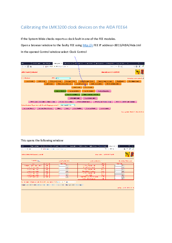
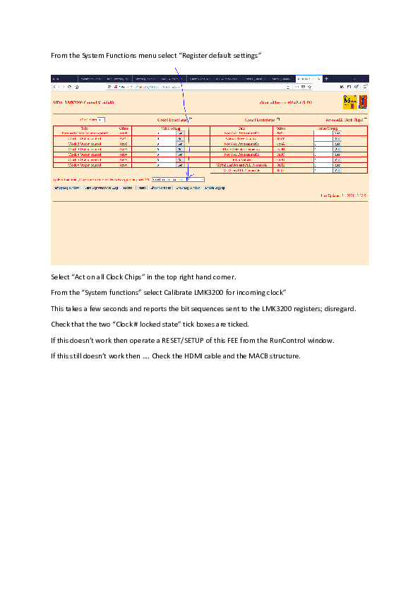
Here is a document showing how and where to calibrate the LMK3200 devices that lock to the system clock and generate the clocks for the ADCs and the FPGA internal logic. |
| Attachment 1: Calibrating_the_LMK3200_clock_devices_on_the_AIDA_FEE64.pdf
|
|
|
210
|
Wed Mar 31 15:40:42 2021 |
PJCS | Check Options files function added |
There is a new operation available in the System Functions menu in the System Wide Checks page. ( The page needs to be reset once when the FEEs are powered before this function will appear )
Check the Options files are all the same size
Using this function will provide a list of the file sizes of the Options/< fee name >/CONTENTS files along with the last time they were accessed as a list.
It's up to the user, at present, to interpret the results but more is possible if required .... |
|
211
|
Wed Mar 31 15:46:09 2021 |
PJCS | HowTo : Synchronize the ASIC clocks. |
To Synchronize the FEE64 ASIC clocks to rise at the same timestamp time use the System function Synchronise the ASIC clocks in the System Wide Checks browser page.
The Server will read the current timestamp value and calculate, based on the number of FEEs and the access delay, a timestamp value sometime in the future. F_stamp
F_stamp is written to each FEE and the synchronization is enabled.
In a state machine in the FEE ASIC clock control, logic is enabled to synchronize its ASIC clock. It compares the current timestamp with F_stamp and if the current timestamp is >= F_stamp then it will start the ASIC clock.
The report in the browser log window gives the 3 LSBs of the timestamp at the instant the ASIC clock is started. They should all be the same. They are from the 10ns timestamp.
|
|
220
|
Wed Apr 14 12:14:47 2021 |
PJCS | Corrections and changes |
14/4/21 @12:00 UK time
Corrected the failure of FADC re-calibration All modules. The problem was a missing > in the .tml file
Edited the sys.tcl file in /MIDAS/TclHttpd/Html/RunControl to comment out where the status of the waveform enable was able to stop the creation of the .W spectra. This will now function at SETUP.
Edited the sys.tcl file to remove the test for Master module at the enable of the Correlation Scalar readout. All modules will now be enabled.
Successfully re-calibrated the LMK3200 in aida09 to remove the clock fault reported in System Wide Checks.
Successfully "sync ASIC clocks" followed by calibrate all module FADCs ( except aida09 which required seperate attention. )
All the Edits first carried out and tested at Daresbury T9 system. |
|
221
|
Wed Apr 14 15:14:55 2021 |
PJCS | Note Well |
Please note that for the forseeable future the system function in the menu on the System Wide Checks browser page labelled as
"Collect the Timestamp RAM values" and "Start the Readout Timestamp error tracing"
Are for the use of engineers only unless otherwise instructed.
There is no harm in using them but the results may be confusing and it is not possible, at present, to detail a definitive set of instructions for their use. |
|
300
|
Fri May 7 19:47:54 2021 |
PJCS | HowTo mitigate excessive temperature in an FEE64 |
After tests in the Daresbury T9 system.
Disabling the waveform ADCs in an FEE64 which is running with the FPGA over temperature will drop the FPGA temperature by 10 degrees.
To disable the ADCs open the Local Control browser window and set the ADC Control register , @2, to 0xFF
The easiest way to restart the waveform ADCs correctly is to rerun SETUP from the control window selecting just the FEE that is affected.
Alternatively STOP acquisition, set the ADC Control register back to 0 and rerun the calibrate ADCs in the FADC Align and Control browser window.
|
|
396
|
Wed Feb 16 10:32:52 2022 |
PJCS | AIDA software changes and some suggestions |
The Pi console monitor program now outputs a full date/time to file for each line of report.
The System Wide Checks has been upgraded to include a check of the PLL lock monitor counters. A baseline is taken when the software starts, or at the users command, then subsequent operation of the command compares the current counter value with the baseline. There are two PLLs on the pcb, LMK3200, and the remainder are in the FPGA. Should there be a disruption in the external clock source to the FEE64 then it is possible the Lock signal from one or more of the PLLs will go false to indicate the PLL is not locked to the input frequency. This transition is counted in the FPGA. If the clock source recovers then this is the only way to understand that a hiatus has occurred.
Noted this morning that the Options file sizes are different and there is no common update date across the 16. I will further improve this function to try and indicate differences ... if required ?
aida07 ADCs will not calibrate. I have attempted to understand why but I have not seen this behaviour before. I suggest, if this is a problem, that a power-cycle be carried out and then the module is replaced if no improvement is noted.
Merger message logging. I have transferred across my version of the New Merger to the npg folder. /home/npg/Patrick/NewMerger. It runs from the command /home/npg/Patrick/NewMerger/MergeServer/bin64/run and is currently set for 16 links. The only changes to the NewMerger code have been made in the message.c file. The rest is untouched.
This version will create a log file directory in /MIDAS/log/Merge_Logs. A new directory structure is created here each time the New Merger is started. The directory is named using the date and a number which refers to the number of times the New Merger has been started on that date. ( /MIDAS/log/Merge_Logs/16_02_22_5 )
Within this directory are text files storing the messages from each of the processes in the New Merger system. The link file messages are stored in a sub-directory as they are currently named by the process number and not the link number. (/MIDAS/log/Merge_Logs/16_02_22_5/links/Link_1529.txt )
The purpose of this change is to be able to correlate error messages reported from the FEE64 consoles with information from the Merger processes.
The system is currently running with this software for the next fortnight. |
|
490
|
Wed Jun 22 10:09:12 2022 |
PJCS | INFO: FEE64 supply Voltages |
Study of the FEE64 power supply distribution has yielded the following :-
The most sensitive regulator, as regards the device voltage input, is the TPS51100 that supplies the DDR memory reference voltages. This requires +4.75 to +5.25 volts. This is supplied from the Power input connector +5v input.
The common LT3080 regulator used over much of the board is a Low Voltage Dropout regulator. This requires 0.5v difference between input and output voltage as minimum. This is not a problem with the +4.75v minimum for the TPS51100 requirement setting the voltage for the board.
The supply to the mezzanine is direct from the power connector +5v input. On the mezzanine there is an LT3080 for each ASIC supplying the required 3.3v. These regulators would possibly benefit from a 1uF capacitor at the Control voltage input.
The simplest approach would be to add a capacitor to the bottom layer where the Control voltage enters the mezzanine.
The power cable has a nominal resistance of 13.3ohms/km. The 3 conductors of the cable are supplying 10A when all is in operation. So the expected voltage drop would thus be ( 10 x 13.3 x 0.007 ) /3 => 0.3v each core.
The conclusion would be that the voltage at the power supply should drop to 5.25 v thus ensuring the TPS51100 is supplied as required regardless of the operation of the FEE.
This will be tested at Daresbury. |
|
514
|
Wed Sep 14 19:07:07 2022 |
PJCS | INFO : Three Merger Statistics explained |
There are three Merger statistics that can be used to better understand how the data flow through the Merger system is proceeding.
Two are from the Link task and one is from the Merger.They are all "No data buffers avaliable" with #1, #2, #3 at the end.
#1: This is incremented when the Link task has a data item to put in the queue for the Merge process but there is no room.
#2: This is incremented when the Link task has found no room in the queue for the Merge process ( #1 ) , waited , tried again and failed.
#3: This the other end of the queue. When the Merge task requests a data item from a Link task queue and there is nothing available.
|
|
225
|
Fri Apr 16 00:47:36 2021 |
OH-ML | AIDA DAQ Reset |
1:18 (CET) No rate in AIDA 07.
Oscar did a AIDA DAQ reset and a quick wide check.
(Power cycle
All back to normal. |
|
1
|
Thu Sep 6 15:11:17 2018 |
OH, TD | Tuesday 4 September - Thursday 6 September |
Attachment 1 - FEE64 temperatures illustrating (we assume) a faulty PSU temperature sensor for aida07

Attachment 2 - FEE64 temperatures following replacement of aida07

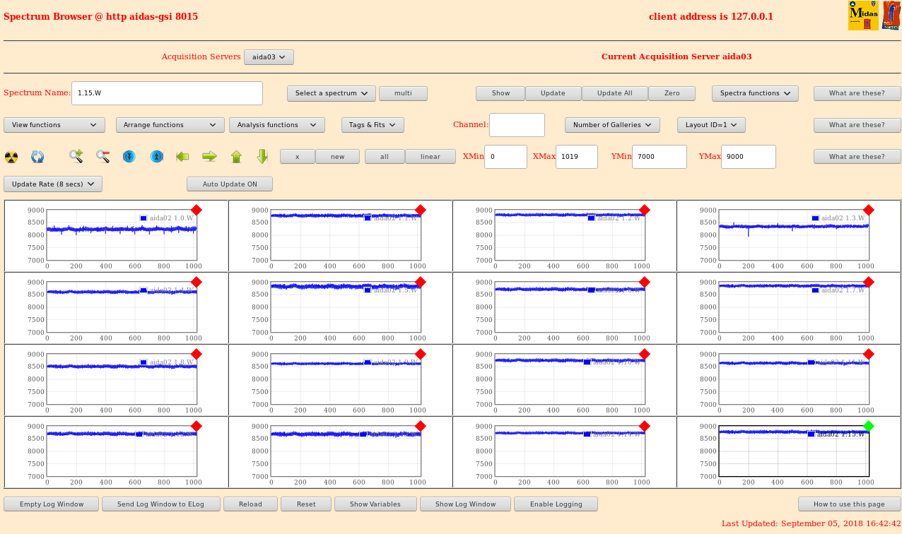
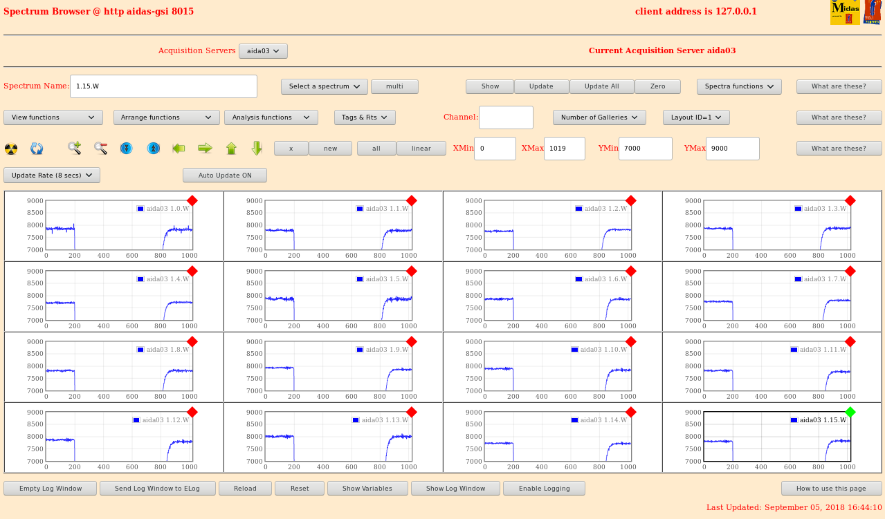
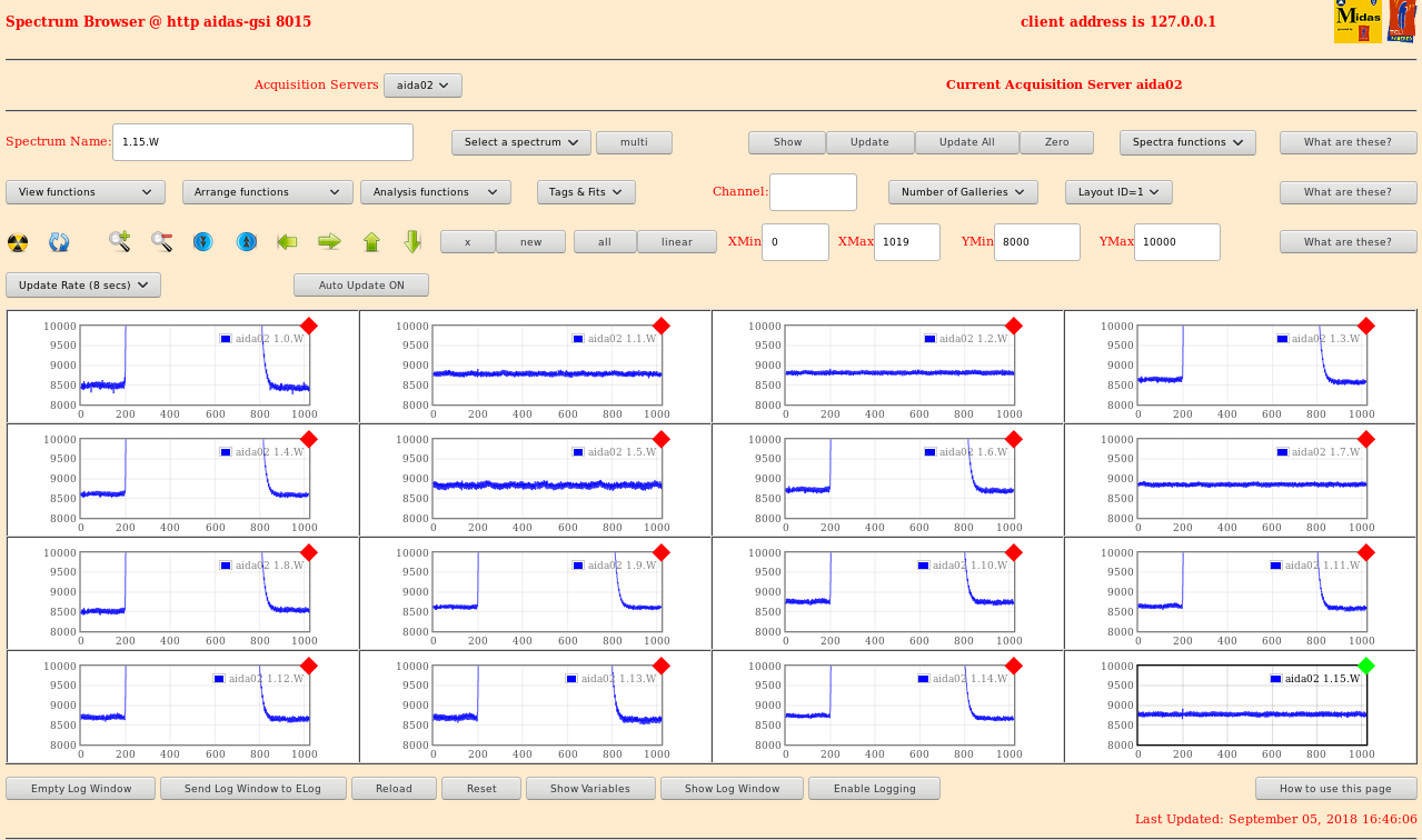
Attachment 3-5 - 1.*.W waveforms for aida01 - aida03 - LED settings for aida02 incorrect, aida01 adaptor PCB
incorrectly aligned

Attachment 6-7 - 1.*.W waveforms for aida02 and aida04

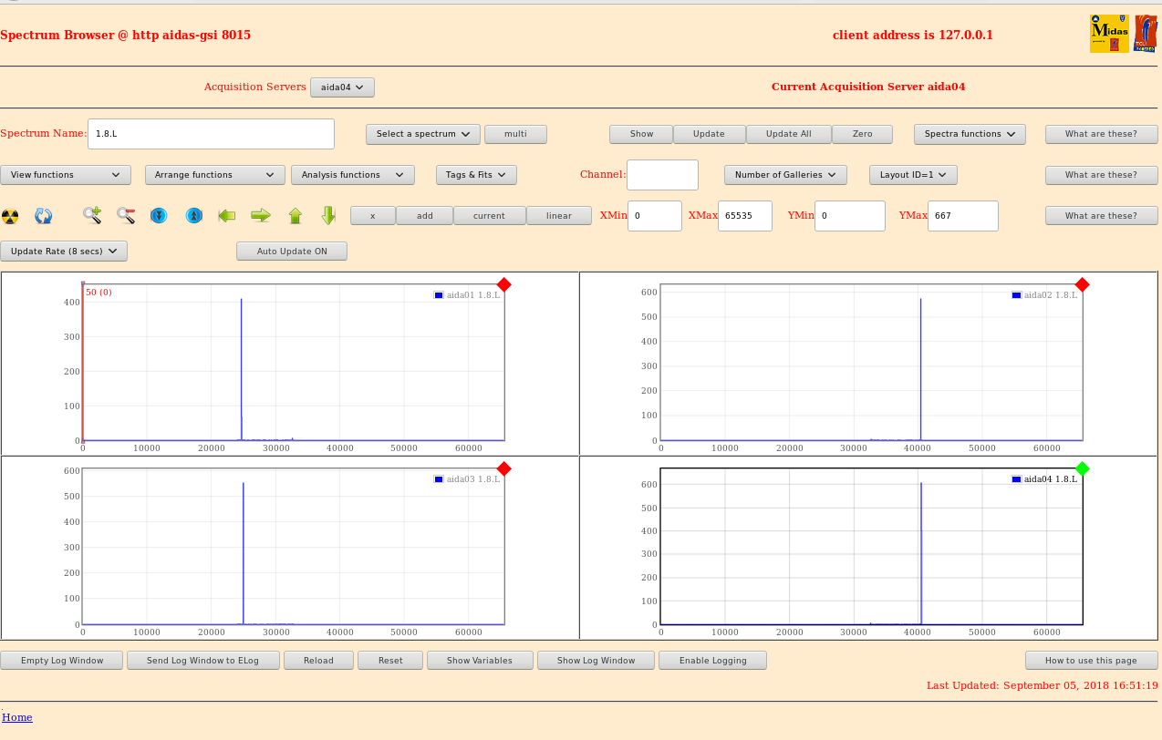
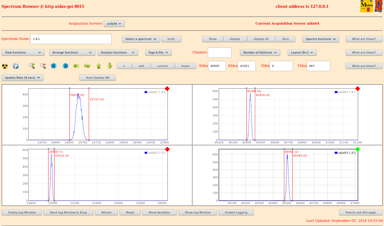
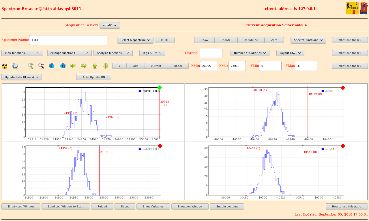
Attachment 8-9 - aida01 - aida04 1.8.L spectra full range and expanded scale
                          pulser peak width c. 15-20 channels FWHM

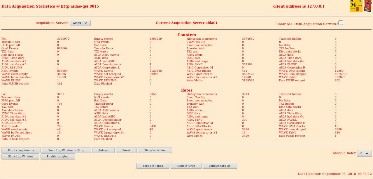
Attachment 10-12 - good events stats for all FEE64s and all statistics for aida01 and aida05
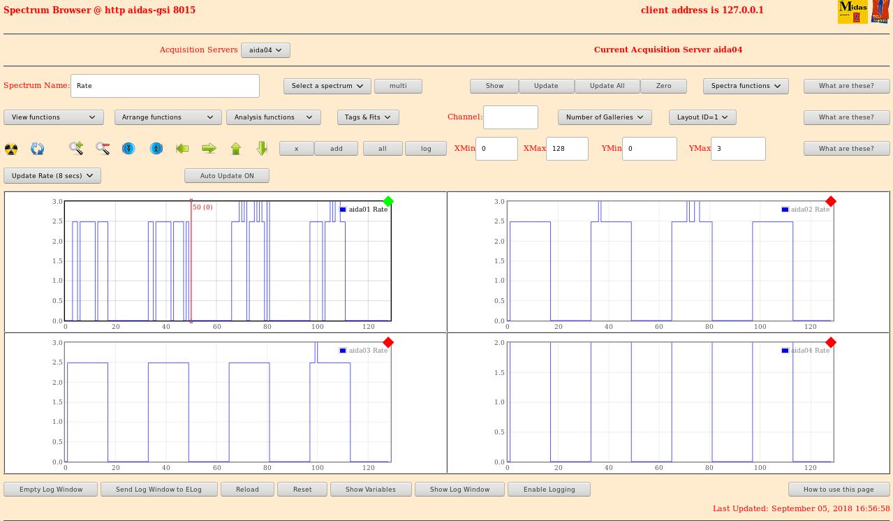
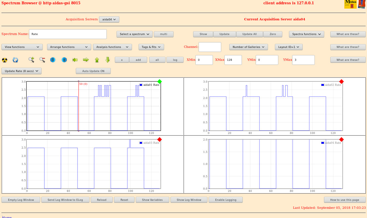
                   Note aida01 - aida04 show rates expected, all other FEE64s show very rates due to noise
                   aida01 - aida04 adaptor PCB are well grounded to FEE64 copper mezzanine/cooling plate, the other
FEE64s are not

Attachment 13-14 - aida01 - aida04 rate spectra before and after correcting alignment of aida01 adaptor PCB

Attachment 15 - aida01 - aida04 1.8.L spectra, expanded scale

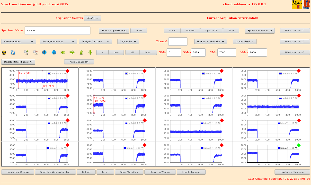
Attachment 16 - illustrates high frequency noise (period 5 samples = 100ns) for aida01 which is not observed for
aida02 - aida03
                subsequently determined that this is not due to a possible adaptor PCB fault by changing the adaptor
PCB
                Note that with bias turned on this noise did appear when Bias was on but all the other groudning
connectors for aida05-aida12
were not in effect.

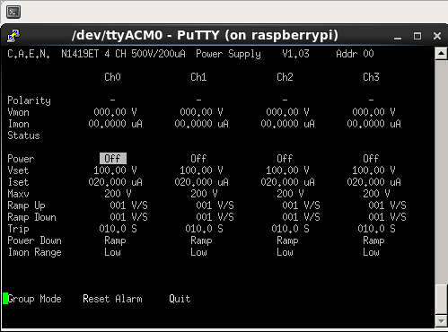
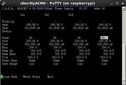
Attachment 17-19 - PuTTY connection to CAEN 1419ET 4ch high voltage supply illustrating PuTTY, N1419ET configuration
and leakage current with 100V applied to adaptor PCBs (no input cabling or DSSSD connected)

Note the CAEN N1419ET appears as a 'USB ACM' device and we connect using /dev/ttyACM<n>. |
| Attachment 1: 180904_1615_FeeTemp.png
|

|
| Attachment 2: 180905_1444_FEETemp.png
|

|
| Attachment 3: 180905_1636_aida01W.png
|

|
| Attachment 4: 180905_1643_aida02W.png
|
|
| Attachment 5: 180905_1644_aida03W.png
|
|
| Attachment 6: 180905_1646_aida02W.png
|
|
| Attachment 7: 180905_1647_aida04W.png
|

|
| Attachment 8: 8_L.png
|
|
| Attachment 9: 8_L_Zoom.png
|
|
| Attachment 10: 180905_1653_Stats.png
|

|
| Attachment 11: 180905_1654_aida01Stats.png
|
|
| Attachment 12: 180905_1654_aida05Stats.png
|

|
| Attachment 13: 180905_1657_HitRateAida1-4.png
|
|
| Attachment 14: 180905_1703_HitRateZoomPostAlign.png
|
|
| Attachment 15: 180905_1707_aida01_1_8_L.png
|
|
| Attachment 16: 180905_1709_aida01W.png
|
|
| Attachment 17: 180906_1424_biasWindow.png
|
|
| Attachment 18: 180906_1425_Putty.png
|

|
| Attachment 19: 180906_1441_BiasOnNoDSSD.png
|
|
|
2
|
Thu Sep 6 15:25:19 2018 |
OH, TD | AIDA@DESPEC Setup Photos |
|