| ID |
Date |
Author |
Subject |
|
80
|
Wed Apr 29 11:00:29 2015 |
TD | Wednesday 29 April 2015 - R20 screenshots |
1230: Attachments

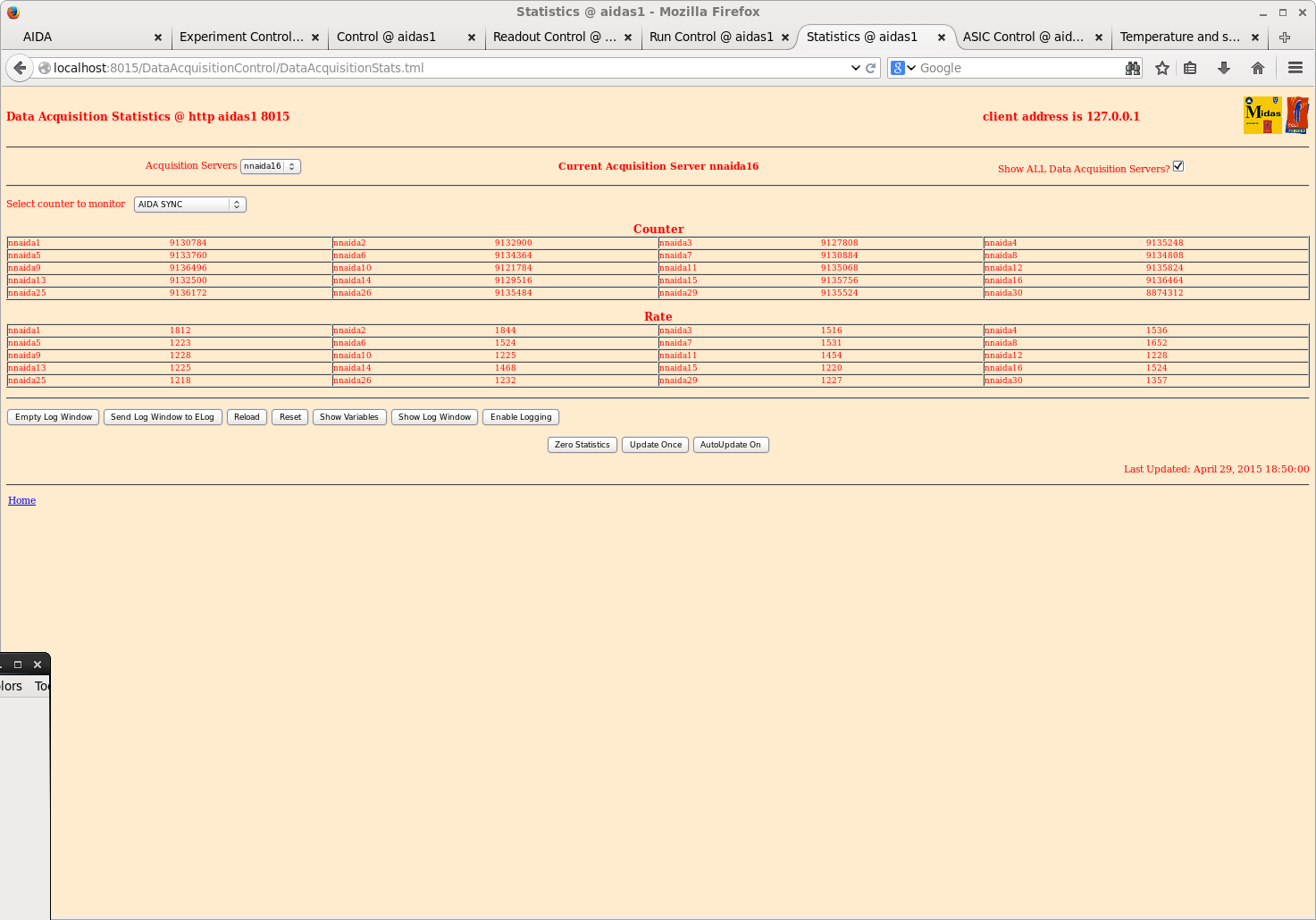
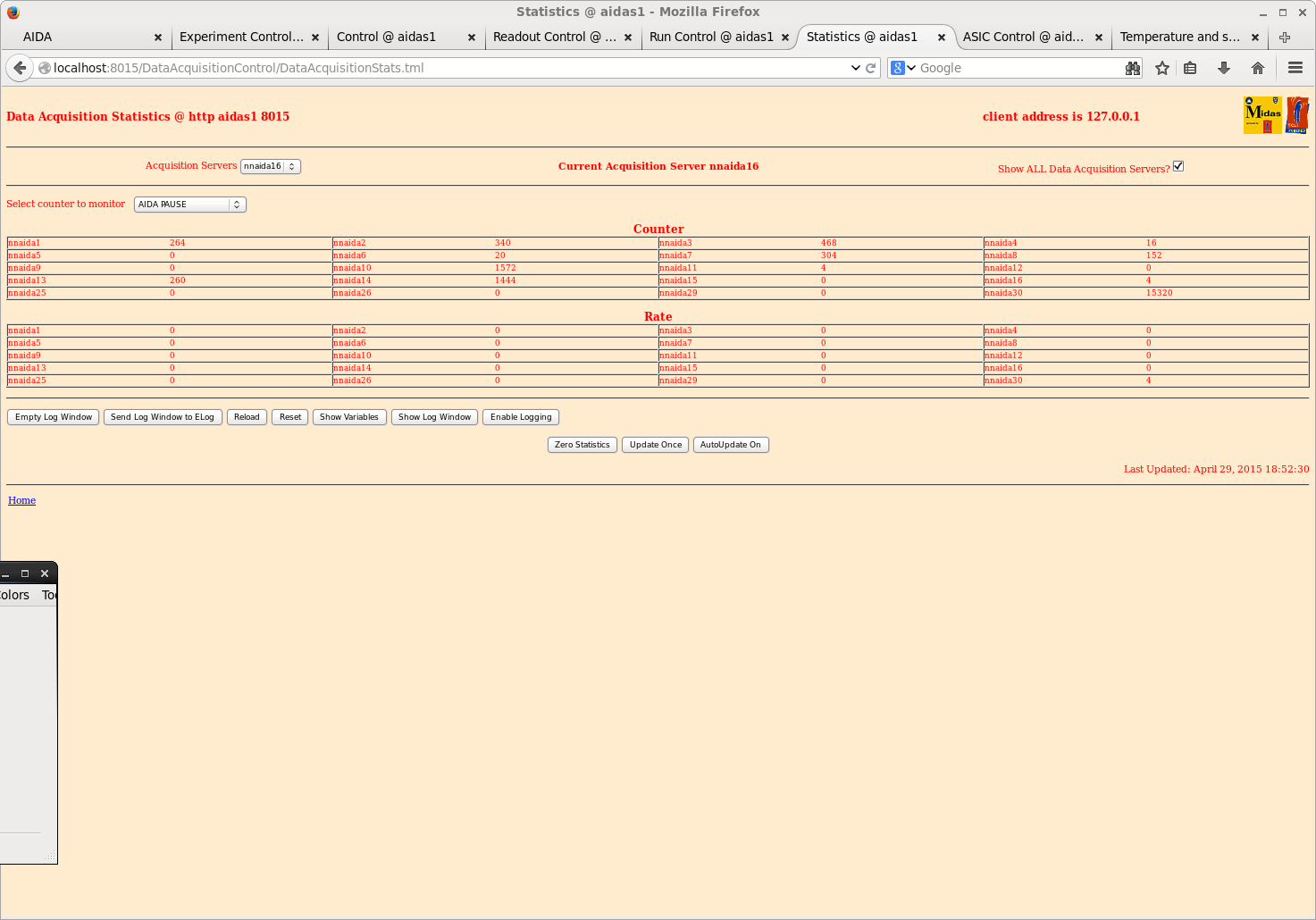
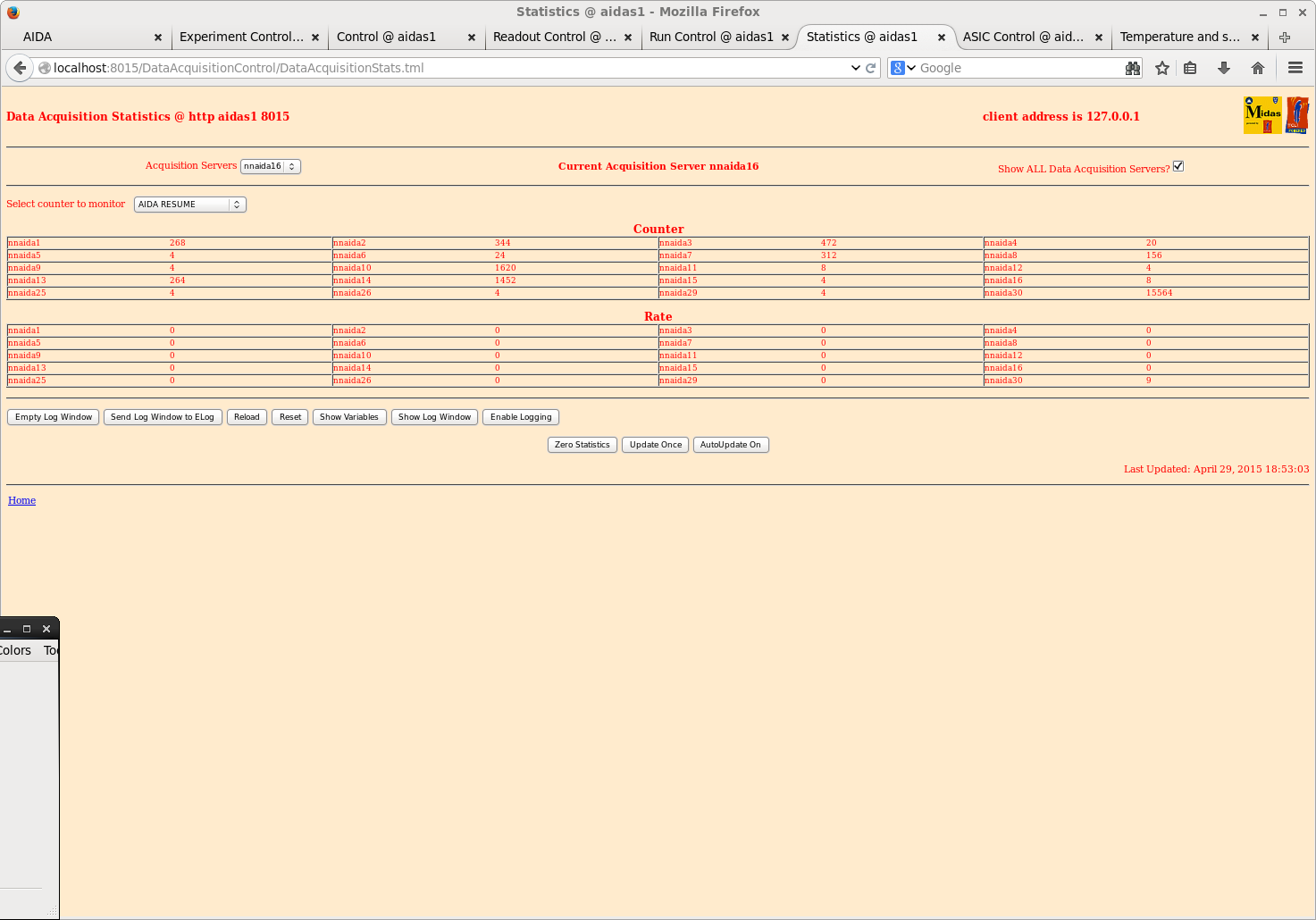
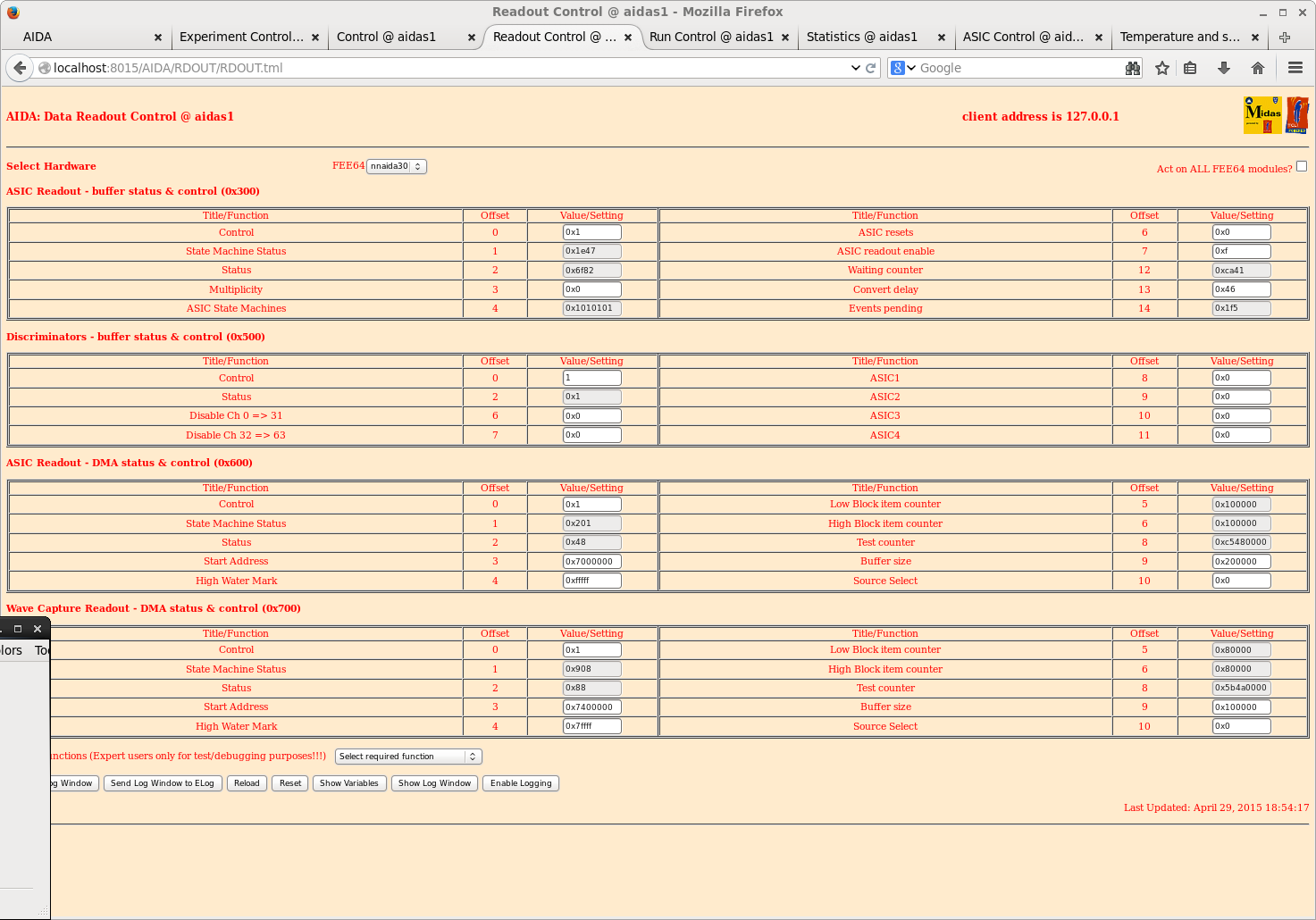
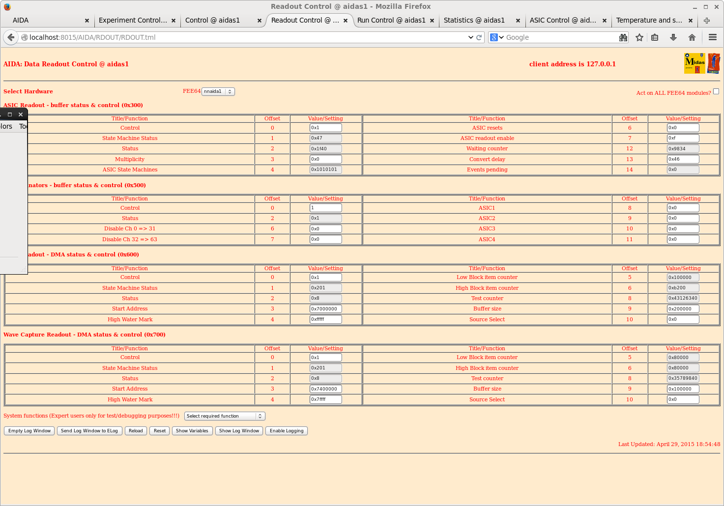
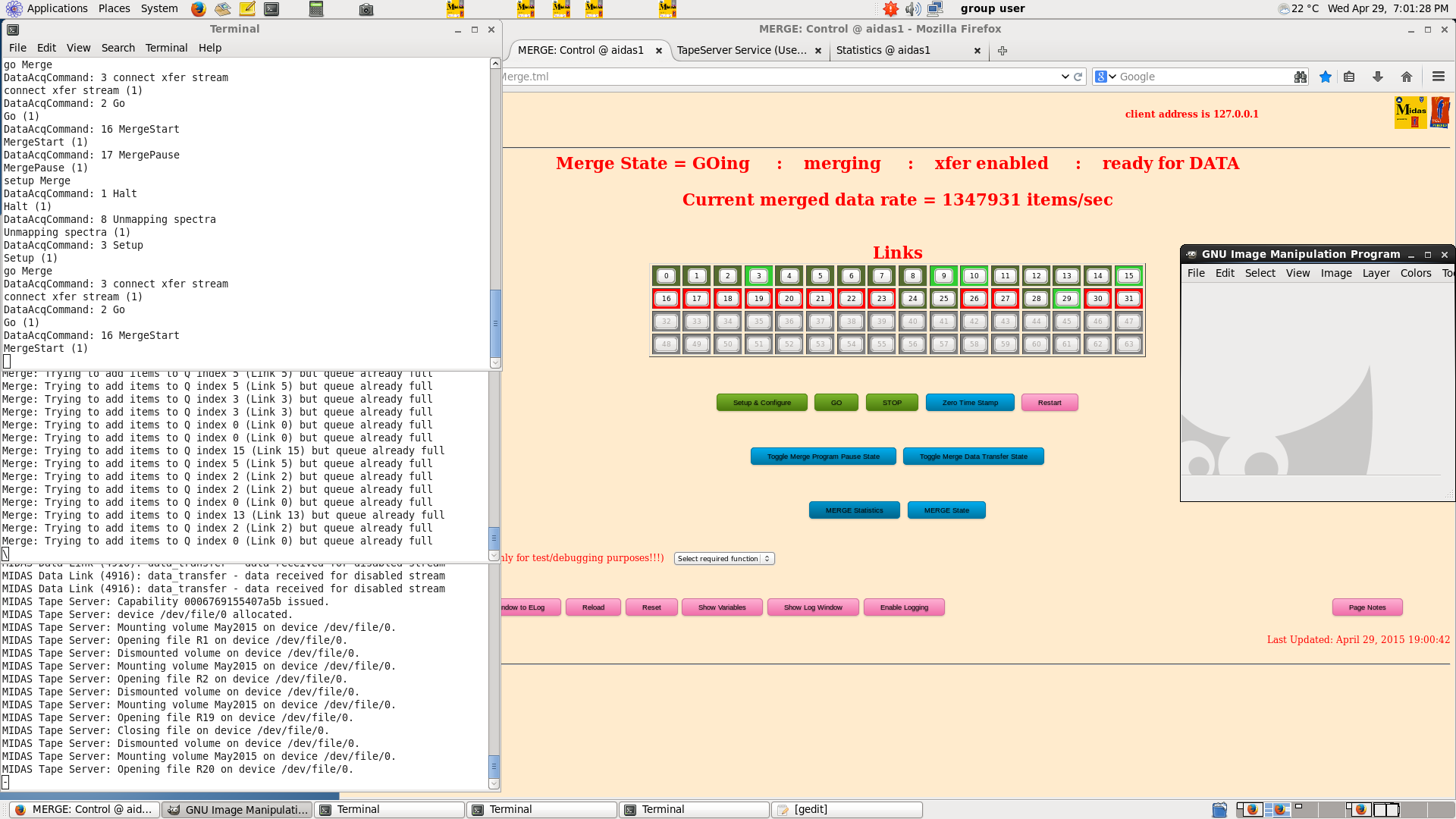
19.00 Screenshots taken during R20 |
| Attachment 1: 40.png
|
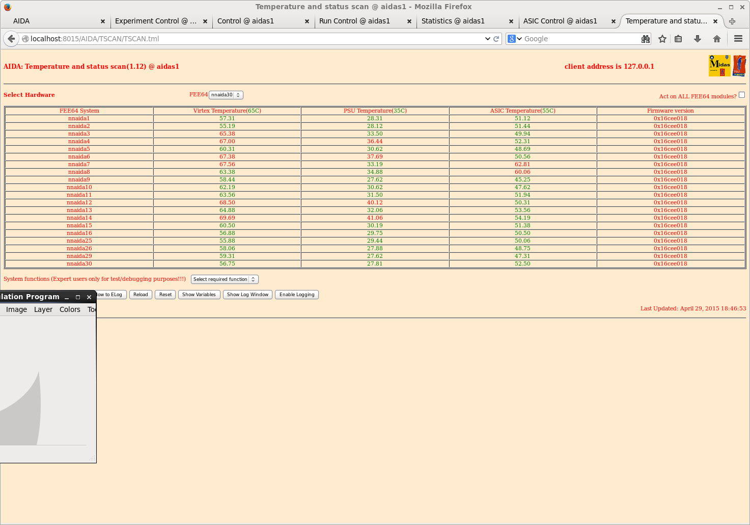
|
| Attachment 2: 41.png
|
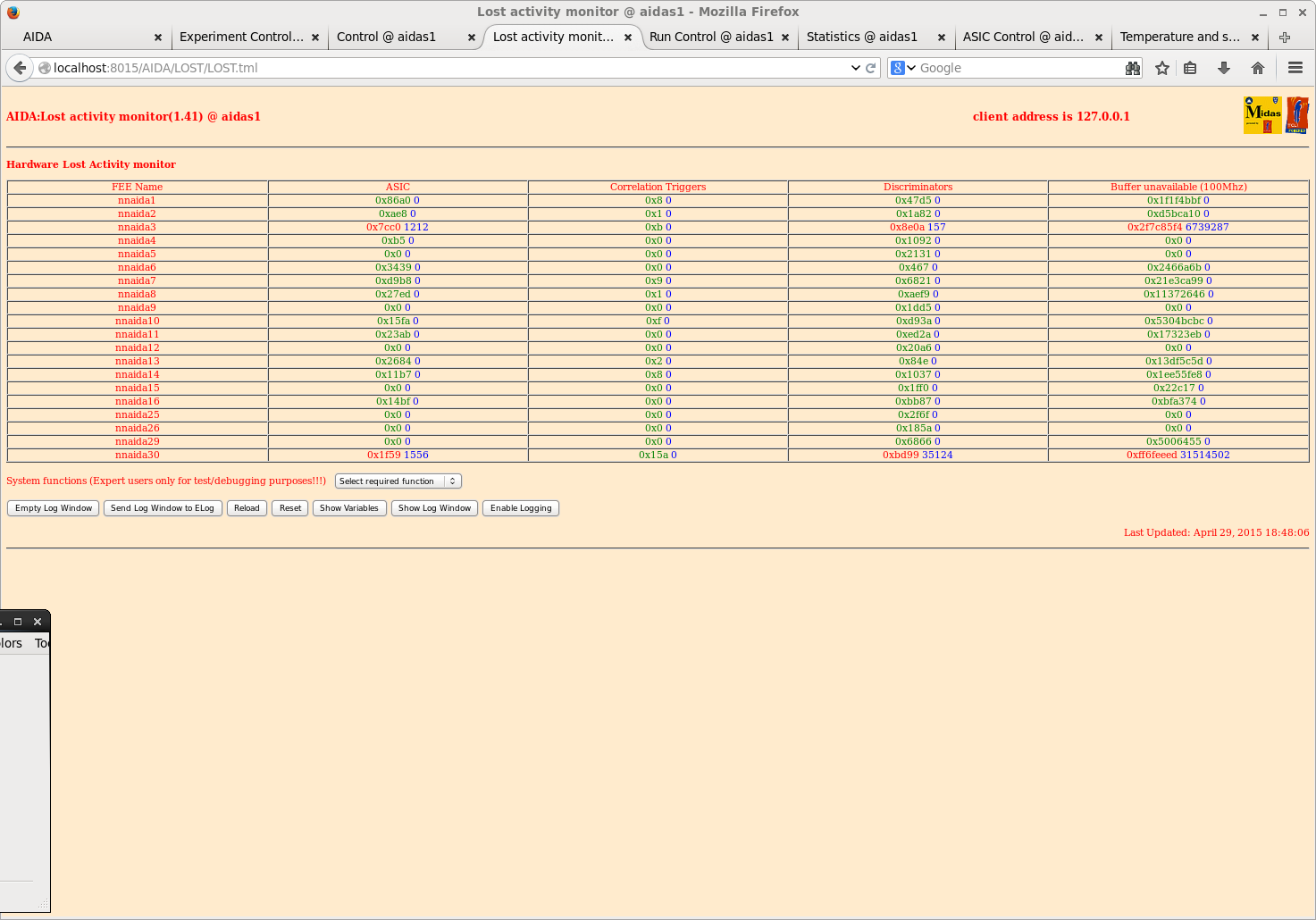
|
| Attachment 3: 42.png
|
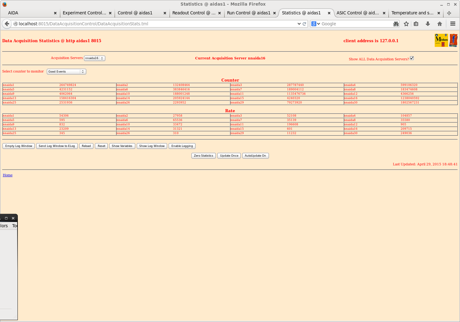
|
| Attachment 4: 43.png
|
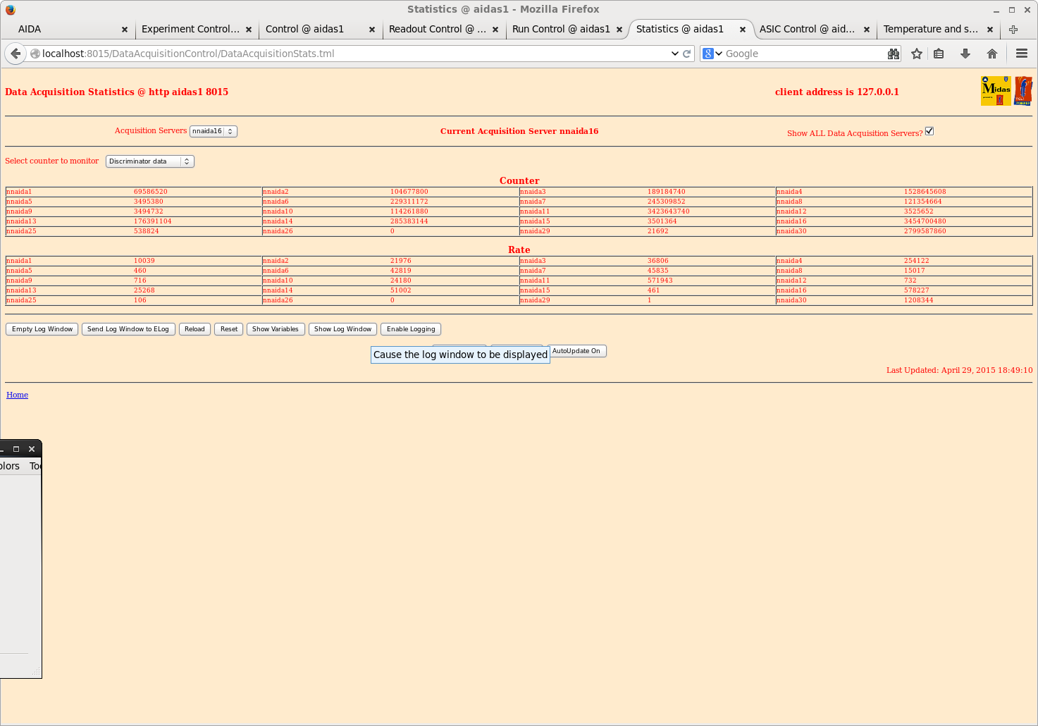
|
| Attachment 5: 44.png
|
|
| Attachment 6: 45.png
|
|
| Attachment 7: 46.png
|
|
| Attachment 8: 47.png
|
|
| Attachment 9: 48.png
|
|
| Attachment 10: 49.png
|
|
|
79
|
Wed Apr 29 10:01:27 2015 |
Patrick Coleman-Smith | Fast Trigger output fault in FEE64 FPGA logic |
The Fast Trigger output of the FEE64 is formed from the OR of the four OR16 signals ( one from each of the ASICs.
The logic levels of the OR16 signals are active low in the FPGA and so if the are OR'd together then the output is inactive if any one of the ASICs is inactive.
This is a problem when the Fast Trigger is being used by other DAQ systems.
A new FPGA program 0x1b4FE01A ( version 26 ) is being compiled.
The Fast Trigger output will provide the logic AND of the four OR16 signals which should give the correct signal. This setting is selected by "Setup".
The other settings available using the Trigger register are shown below. Note that OR64 is the logic OR of the masked outputs of the ASIC individual Discriminator outputs.
when 0 =>
trigger_hit <= ASIC1_data_ready ;
when 1 =>
trigger_hit <= ASIC1_rdo_range and ASIC1_data_ready ;
when 2 =>
trigger_hit <= ASIC2_rdo_range and ASIC2_data_ready ;
when 3 =>
trigger_hit <= led_trigger(0) ;
when 4 =>
trigger_hit <= led_raw(0) ;
when 5 =>
trigger_hit <= chan_reset(0) ;
when 6 =>
trigger_hit <= force_capture_sync ;
when 7 =>
trigger_hit <= force_capture ;
when 8 =>
trigger_hit <= ASIC1_OR_16 ;
when 9 =>
trigger_hit <= ASIC2_OR_16 ;
when 10 =>
trigger_hit <= ASIC3_OR_16 ;
when 11 =>
trigger_hit <= ASIC4_OR_16 ;
when 12 =>
trigger_hit <= ASIC4_OR_16 and ASIC3_OR_16 and ASIC2_OR_16 and ASIC1_OR_16;
when 13 =>
trigger_hit <= led_trigger(1) ;
when 14 =>
trigger_hit <= OR64 ;
when 15 =>
trigger_hit <= ASIC4_OR_16 or ASIC3_OR_16 or ASIC2_OR_16 or ASIC1_OR_16; |
|
78
|
Wed Apr 29 01:03:41 2015 |
JA, LHB, TD, AE, CG & VP | Wednesday 29 April 2015 |
Overnight
      Beam tuning, PID tests - beam stopped in scintilator detector + 1" thick Pb bricks
      DAQ ran OK (not to disk)
      DSSSD #3 tripped, re-enabled OK


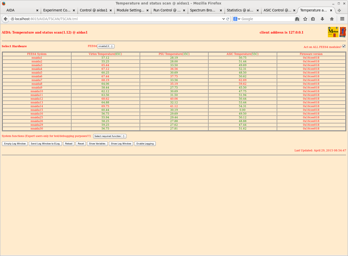
09.00 AIDA temperatures - attachment 1
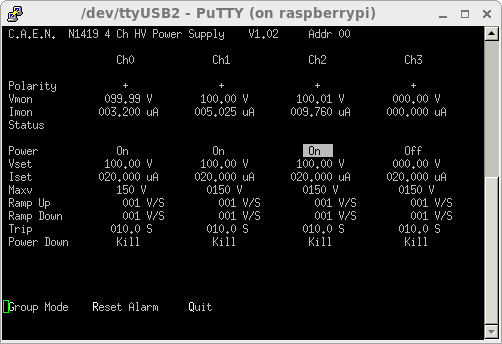
      CAEN N1419 HV settings - attachment 2

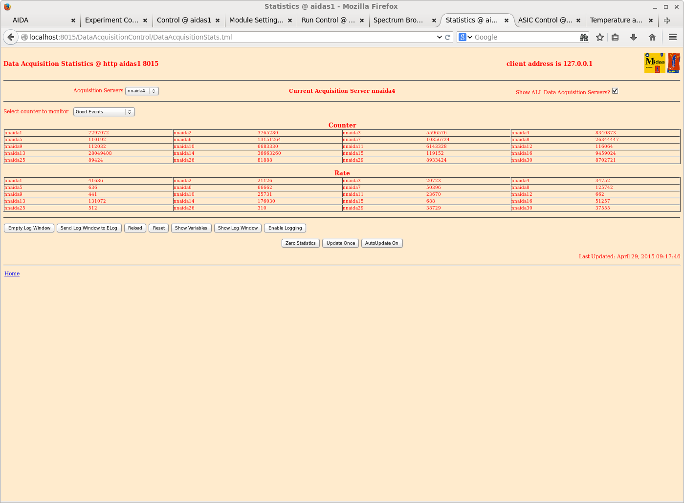
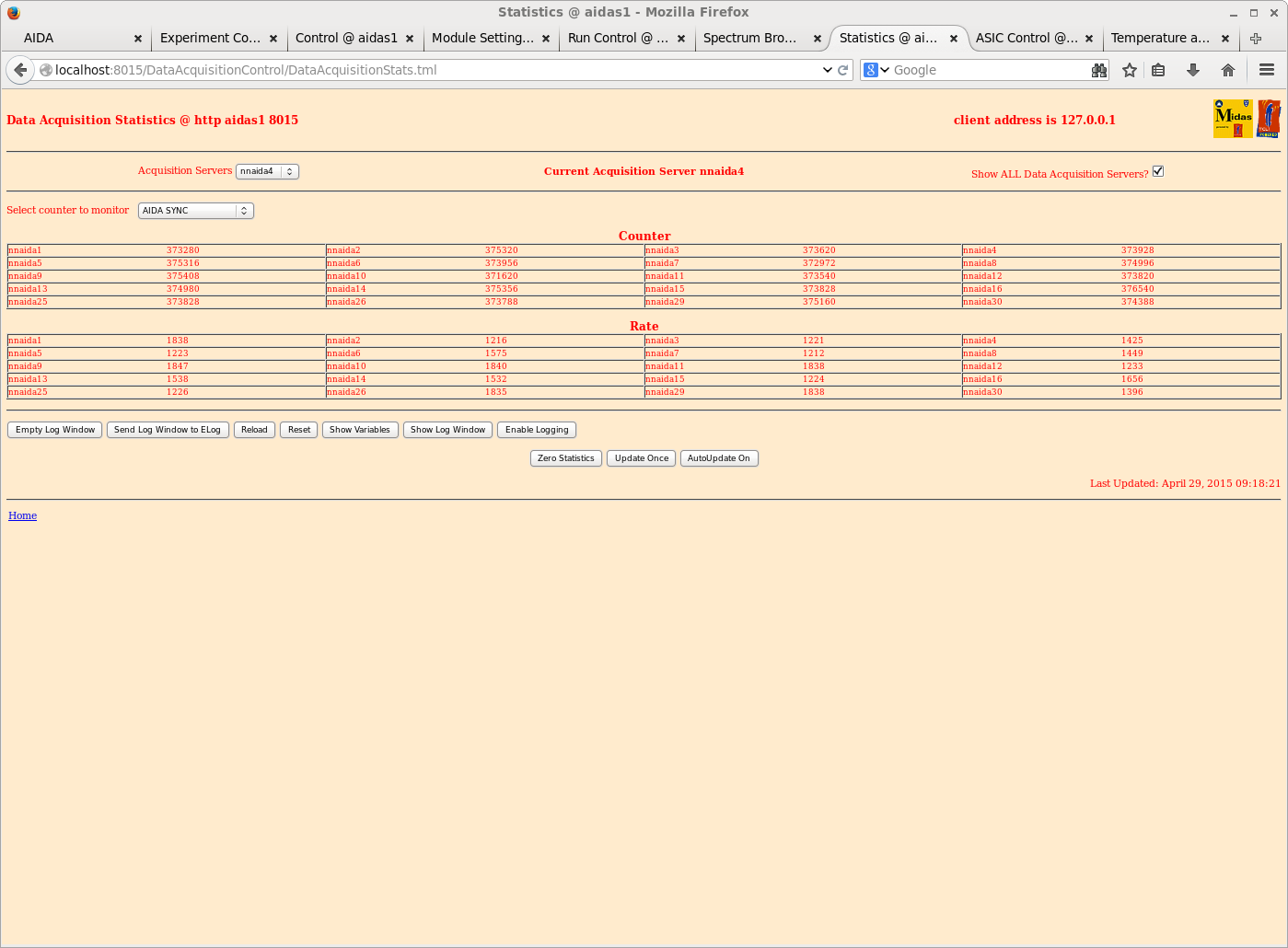
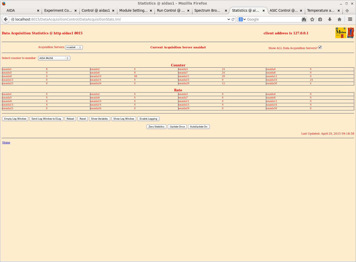
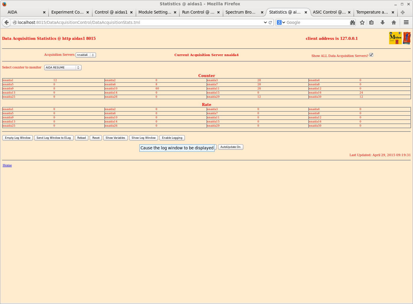
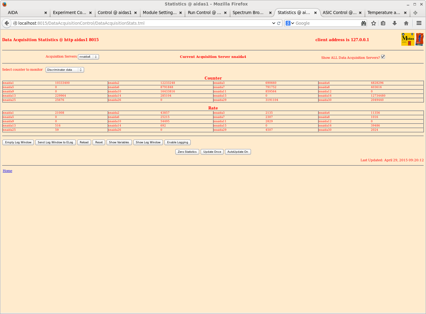
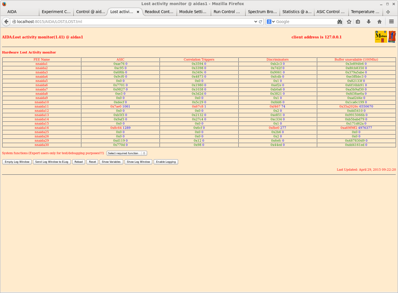
09.25 Statistics & lost activity - attachments 3-8

10.30 Scintilator detector + 1" thick Pb bricks removed
      ~1KHz 84Zn to Degrader + MICA + Veto + AIDA DSSSDs #1-3 + 10mm Al

      Data file R15 12.15-12.59 beam lost
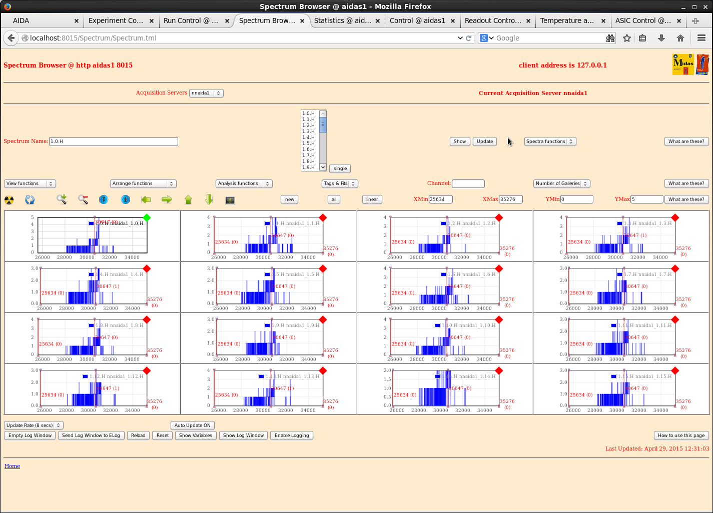
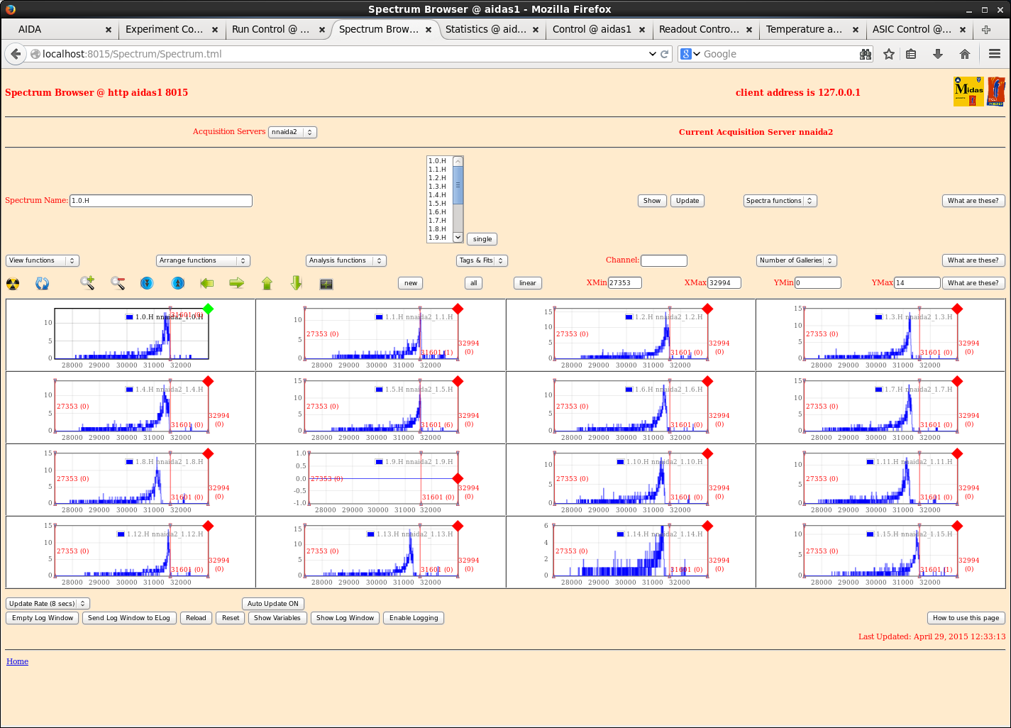
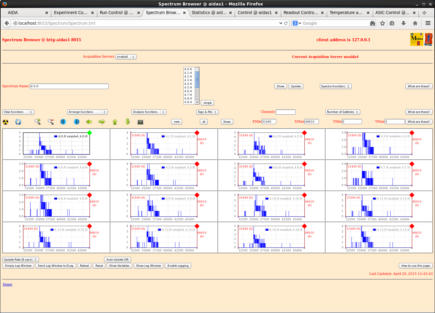
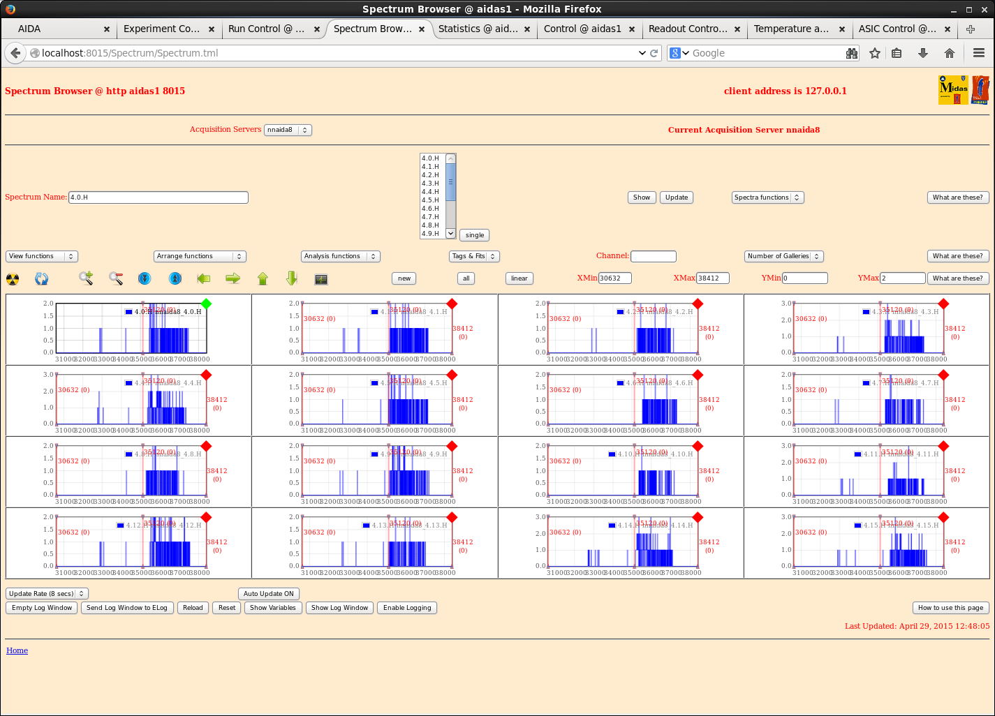
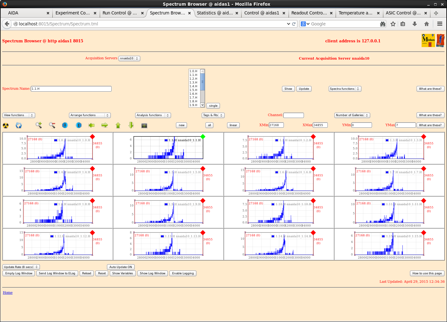
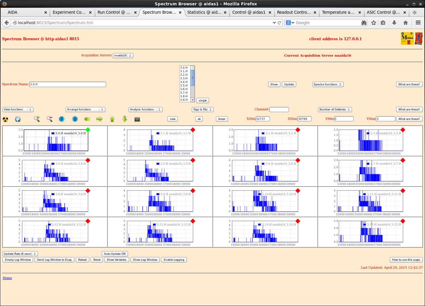
      Attachments 9-14 DSSSD #1-3 HEC ADC spectra, HEC LLD 0x08

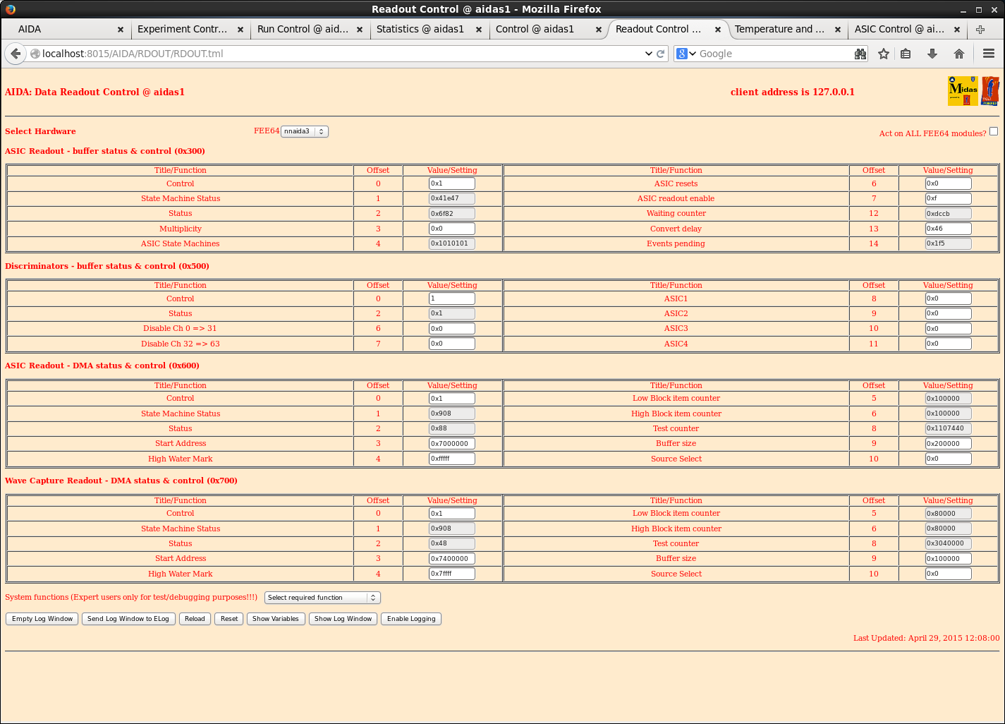
      Attachments 15-16 Examples of Data Readout Control following stalled DAQ GO (no SYNCs)

      Data file R16 13.02-13.46 SYNCs lost/MERGE stalled
      HEC LLD 0x02

      Data file R17 13.46-14.20

      Data file R19 15.30-17.05

      Data file R20 17.06
      Fast comparator LLD HEC 0x02, LEC 0x20 (except nnaida30 HEC 0x20)

22.14 Data file R22 22.14 - 30.4.15 09.00
      Now using /data20/TapeData/May2015 to store data
      Spectra cleared at start of run
      DAQ OK, CAEN N1419 ch #2 tripped
|
| Attachment 1: 31.png
|
|
| Attachment 2: 32.png
|
|
| Attachment 3: 33.png
|
|
| Attachment 4: 34.png
|
|
| Attachment 5: 35.png
|
|
| Attachment 6: 36.png
|
|
| Attachment 7: 37.png
|
|
| Attachment 8: 38.png
|
|
| Attachment 9: 20150429_nnaida1_det3_H.png
|
|
| Attachment 10: 20150429_nnaida2_det2_H.png
|
|
| Attachment 11: 20150429_nnaida4_det2_H.png
|
|
| Attachment 12: 20150429_nnaida8_det3_H.png
|
|
| Attachment 13: 20150429_nnaida10_det1_H.png
|
|
| Attachment 14: 20150429_nnaida16_det1_H.png
|
|
| Attachment 15: 20150429_dataReadout_nnaida4.png
|

|
| Attachment 16: 20150429_datrareadout_nnaida3.png
|
|
|
77
|
Tue Apr 28 11:22:25 2015 |
VP | RPI |
replace RPI with model B+. 4 USB ports + 4 port switch
The RPI system has been replaced by a model B+ which has 4 internal USB ports
Connects to:
AIDA Power Control USB1
Serial port to FEE for console output USB0
CAEN N1419 HV power supply USB2
All 3 connections use a USB => RS232 convert chip. The hardware cannot simply tell these apart. The USB ports assigned should however remain constant as long as the connections remain the same.
Power up RPI system.
At end of boot check the last couple of lines on the console for the assigned IP address. Should be 10.1.1.114.
login using ID npg Password is the same as for the data acq system.
then type startx
When the graphical console appears.
Firstly click on the icon TclHttpd Server to start the web server.
Start the web browser (Icon immediately to the right of the MENU icon at extreme left of the top row).
Connect to http://localhost:8015/AIDA/Rly16/Rly16.tml (the browser will have this in its recently used list)
The software now checks the potential USB devices for one which responds correctly to a request for the firmware in the AIDA Power Control box.
The GUI shows the port in use. Currently it is /dev/ttyUSB1
Even if the hardware changes the software should find the correct port to use but this suggests the other uses will also have changed (you may need to use dmesg to locate which ports are assigned)
You can use the icon PuTTY Client to start the putty program.
connect and open for USB0 to monitor the FEE64 console
connect and open for USB2 to control the CAEN N1419
You can connect from a remote terminal using ssh -X -l npg nnrpi1
However to start putty from the command line you will need
sudo chmod 660 /dev/ttyUSB0; putty (for the FEE console)
or
sudo chmod 660 /dev/ttyUSB2; putty (for the N1419 control)
|
|
76
|
Tue Apr 28 06:25:13 2015 |
JA, LHB, TD, AE & CG | Tuesday 28th April progress |
28/04/15
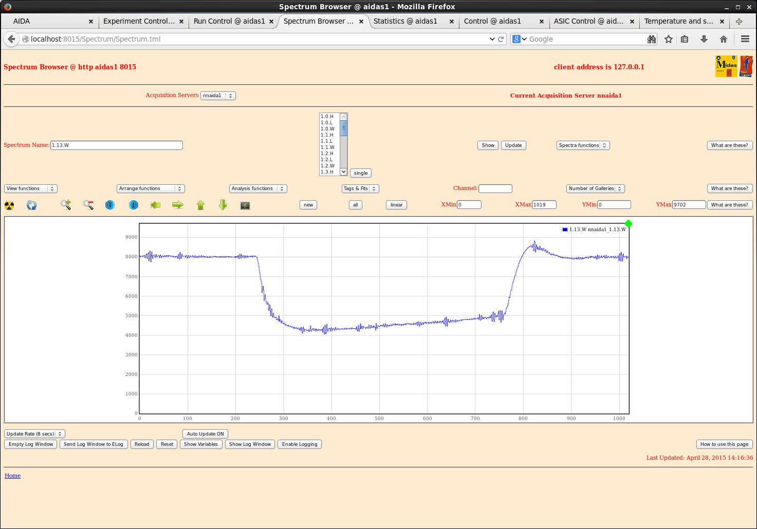
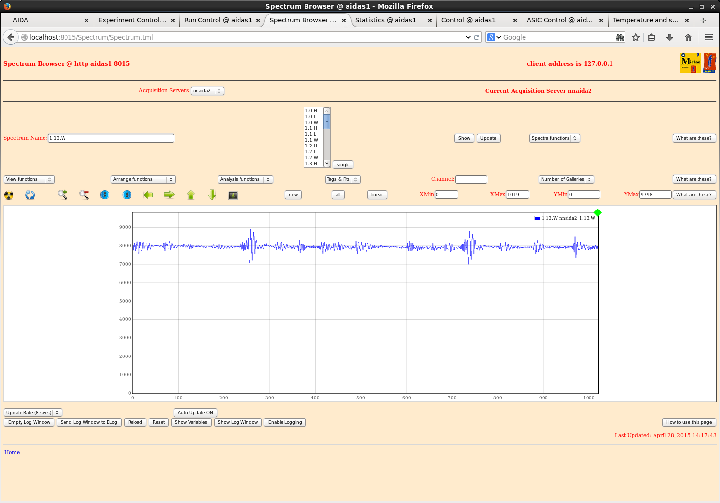
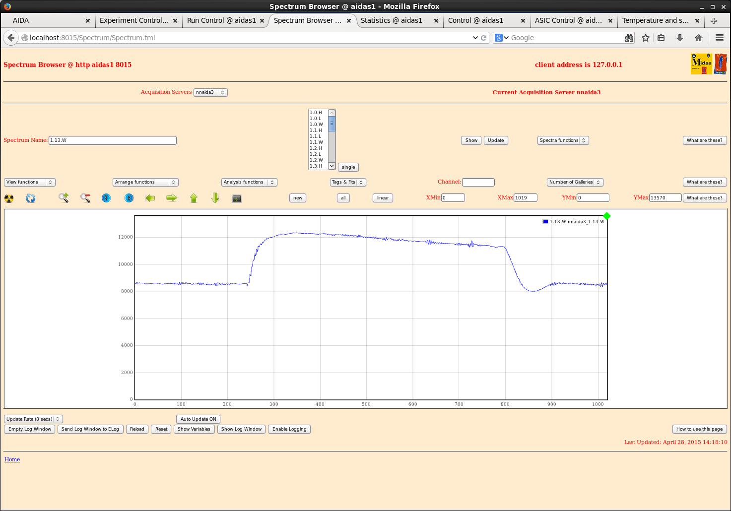
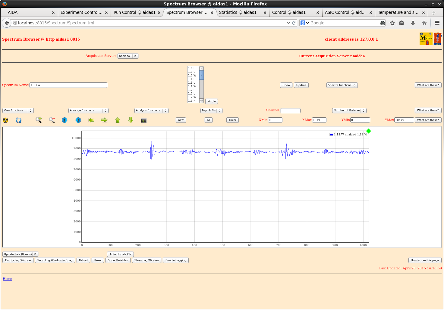
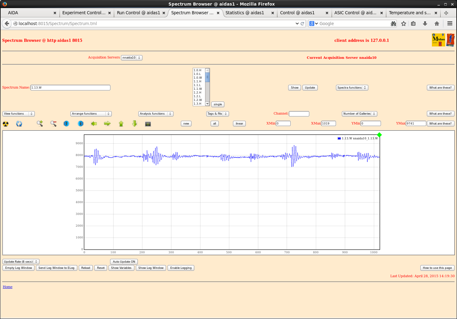
1420: Carried out ASIC optimisation tests to find best shaping time. Chose system wide shaping time of 0x6.
Waveforms of example FEEs/channels attachments 1-6.
20.34 Pulser walkthough - data file /TapeData/May2015/R14_0
BNC PB_4 settings
90,000 - 10,0000 @ 10,000 step
t_r = 50ns, tau_d = 50us
- polarity
x10 attenuator in
tail pulse, delay min, int ref
frequency 250Hz |
| Attachment 1: 20150428_nnaida1_w.png
|
|
| Attachment 2: 20150428_nnaida2_w.png
|
|
| Attachment 3: 20150428_nnaida3_w.png
|
|
| Attachment 4: 20150428_nnaida4_w.png
|
|
| Attachment 5: 20150428_nnaida10_w.png
|
|
| Attachment 6: 20150428_nnaida16_w.png
|

|
|
75
|
Tue Apr 28 05:59:48 2015 |
AE | "beta" trigger from MACB Trigger outputs |
We've constructed a beta trigger with the signals from the p-side of the three DSSDs (OR of all fast
discriminator channels of each FEE).

det1 -> NNAIDA#6 -> MACB#10.2
det1 -> NNAIDA#10 -> MACB#3.4
det2 -> NNAIDA#2 -> MACB#10.3
det2 -> NNAIDA#14 -> MACB#3.2
det3 -> NNAIDA#1 -> MACB#10.4
det3 -> NNAIDA#13 -> MACB#3.3

beta-trigger is OR of all above MACB trigger outputs. Diagram for logic circuit is in paper logbook.


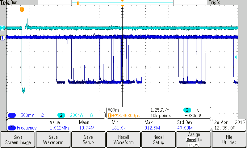
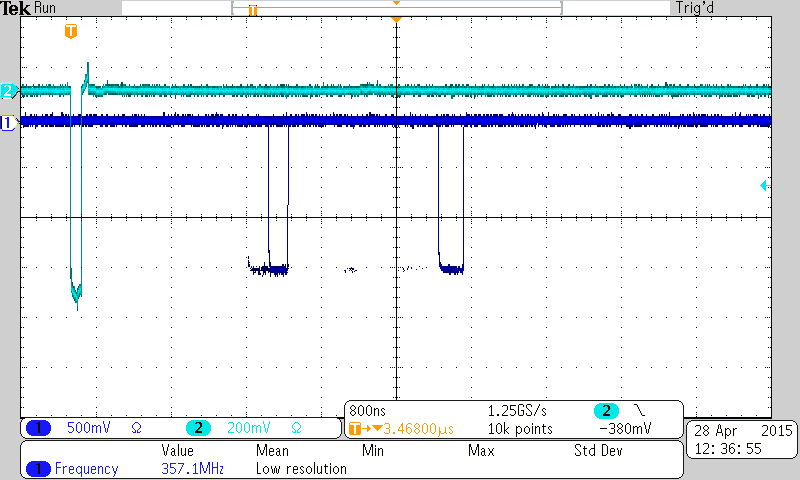
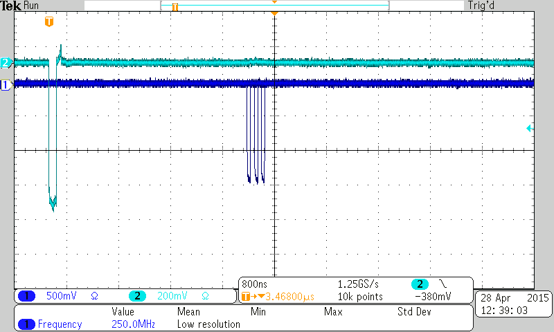
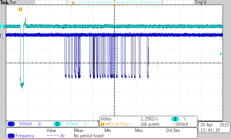
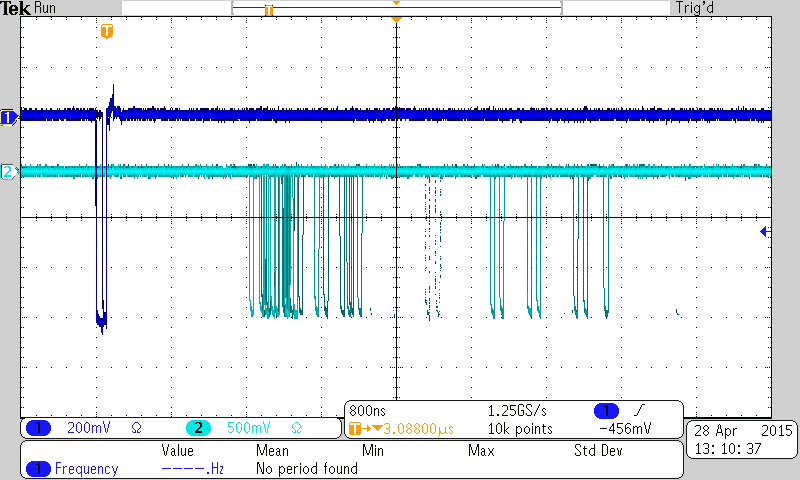
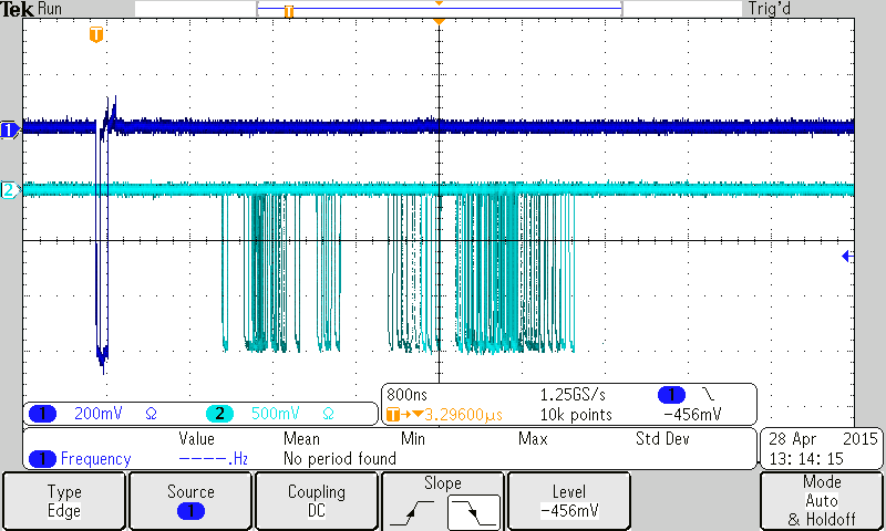
Bellow are some oscilloscope sceenshots. Some things to note about the MACB trigger outputs:

- all show multiple outputs for each pulser input. Some channels seem to have higher level for such 'multiplicity'.

- the width of the outputs varies for different channels (from ~40 ns to ~300 ns)

- the delay between the pulser signal and the output from the MACB is quite large, and also different for each
MACB (measured from ~800 ns up to 2 usec).


Scope screenshots:

 - light blue is the trigger output from Pulser
 - dark blue is output from trigger channel of MACB

 MACB#10.2: tek00001.tif
 MACB#3.4: tek00002.tif
 MACB#10.3: tek00005.tif
 MACB#3.2: tek00007.tif
 MACB#10.4: tek000011.tif
MACB#3.3: tek000018.tif |
| Attachment 1: tek00001.tif
|
|
| Attachment 2: tek00002.tif
|
|
| Attachment 3: tek00005.tif
|
|
| Attachment 4: tek00007.tif
|
|
| Attachment 5: tek00011.tif
|
|
| Attachment 6: tek00018.tif
|
|
|
74
|
Mon Apr 27 04:54:02 2015 |
VFEP & TD | [How To] Remote control of CAEN N1419 Programmable HV Power Supply |
@ CAEN N1419

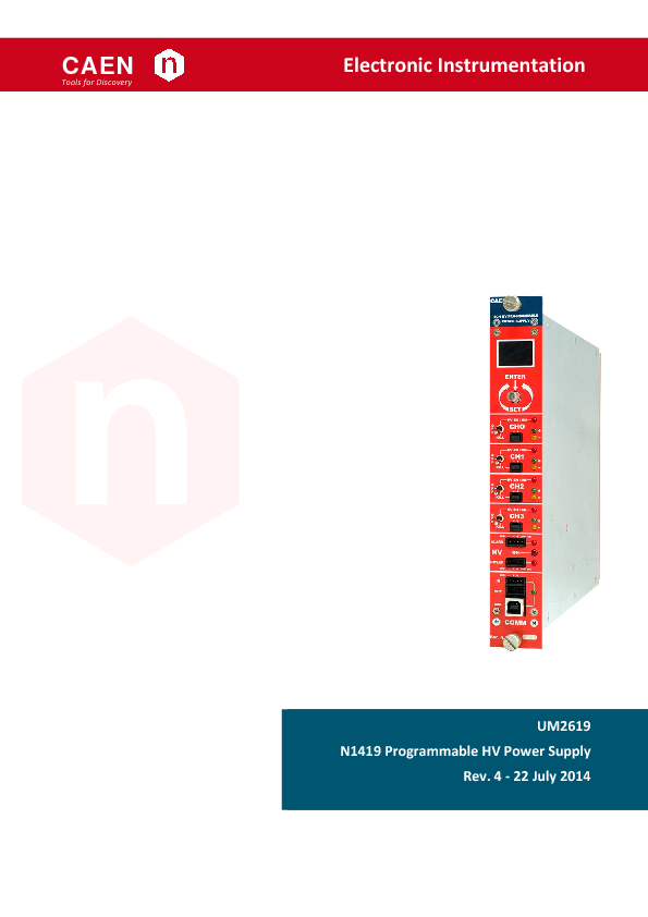
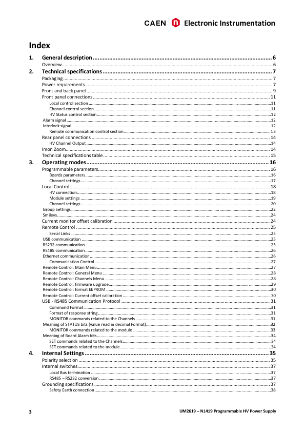
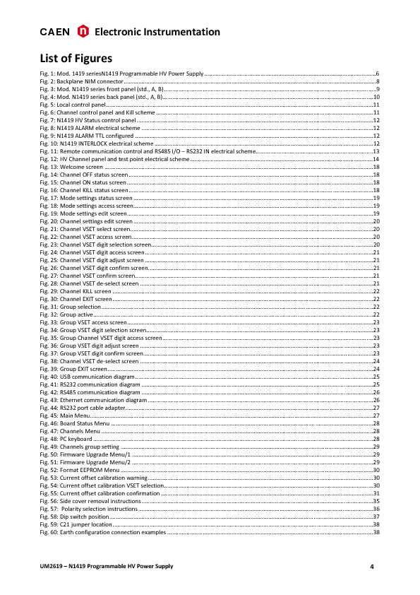
Set programmable parameters - see CAEN N1419 manual p.16 (attachment 1)

INTERLOCK = CLOSED
CONTROL = REMOTE

Set front panel switches HV on/off/kill = ON
No interlock jumpers


@ AIDA server

From a command terminal, login to nnrpi1 using ssh, set device permissions, and launch putty.

ssh -X nnrpi1 -l npg
password:
    :
    :
    :
% sudo chmod 777 /dev/ttyUSB2
% putty &

From the putty window sequentially select 'USB2', 'load' and 'open' - this will select
and load a saved serial session for device /dev/ttyUSB2 and launch a command terminal
for the serial session.

Enter the command 'caen' followed by return. Note the command is not echoed.

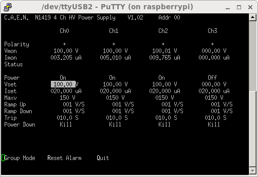
The CAEN HV interface should appear. Enter the command 'd' to display/modify parameters.
See CAEN N1419 manual pp.27-29 for further commands. See attachment 2.

N.B. The above procedure assumes:

/dev/ttyUSB0 = USB-controlled ac mains switch      (device pl2303)
/dev/ttyUSB1 = serial link to FEE64 system console (device FT232RL)
/dev/ttyUSB2 = CAEN N1419                          (device FT232BM)

However, these assignments may vary. You can use the command dmesg to check assignments.
For example,

% dmesg | grep usb
[    1.178926] usbcore: registered new interface driver usbfs
[    1.184722] usbcore: registered new interface driver hub
[    1.190218] usbcore: registered new device driver usb
[    1.568604] usbcore: registered new interface driver smsc95xx
[    2.065233] dwc_otg bcm2708_usb: DWC OTG Controller
[    2.075294] dwc_otg bcm2708_usb: new USB bus registered, assigned bus number 1
[    2.087646] dwc_otg bcm2708_usb: irq 32, io mem 0x00000000
[    2.115566] usb usb1: New USB device found, idVendor=1d6b, idProduct=0002
[    2.127464] usb usb1: New USB device strings: Mfr=3, Product=2, SerialNumber=1
[    2.139731] usb usb1: Product: DWC OTG Controller
[    2.149477] usb usb1: Manufacturer: Linux 3.18.7+ dwc_otg_hcd
[    2.160291] usb usb1: SerialNumber: bcm2708_usb
[    2.190521] usbcore: registered new interface driver usb-storage
[    2.348492] usbcore: registered new interface driver usbhid
[    2.360241] usbhid: USB HID core driver
[    2.677666] usb 1-1: new high-speed USB device number 2 using dwc_otg
[    2.897985] usb 1-1: New USB device found, idVendor=0424, idProduct=9514
[    2.910008] usb 1-1: New USB device strings: Mfr=0, Product=0, SerialNumber=0
[    3.217656] usb 1-1.1: new high-speed USB device number 3 using dwc_otg
[    3.327968] usb 1-1.1: New USB device found, idVendor=0424, idProduct=ec00
[    3.340138] usb 1-1.1: New USB device strings: Mfr=0, Product=0, SerialNumber=0
[    3.422390] smsc95xx 1-1.1:1.0 eth0: register 'smsc95xx' at usb-bcm2708_usb-1.1, smsc95xx USB 2.0 Ethernet,
b8:27:eb:0b:f6:73
[    3.517666] usb 1-1.3: new full-speed USB device number 4 using dwc_otg
[    3.630124] usb 1-1.3: New USB device found, idVendor=067b, idProduct=2303
[    3.642534] usb 1-1.3: New USB device strings: Mfr=1, Product=2, SerialNumber=0
[    3.655514] usb 1-1.3: Product: USB-Serial Controller D
[    3.666257] usb 1-1.3: Manufacturer: Prolific Technology Inc.
[    3.761138] usb 1-1.4: new low-speed USB device number 5 using dwc_otg
[    3.894746] usb 1-1.4: New USB device found, idVendor=046d, idProduct=c016
[    3.908414] usb 1-1.4: New USB device strings: Mfr=1, Product=2, SerialNumber=0
[    3.922059] usb 1-1.4: Product: Optical USB Mouse
[    3.933904] usb 1-1.4: Manufacturer: Logitech
[    3.955374] input: Logitech Optical USB Mouse as
/devices/platform/bcm2708_usb/usb1/1-1/1-1.4/1-1.4:1.0/0003:046D:C016.0001/input/input0
[    3.976035] hid-generic 0003:046D:C016.0001: input,hidraw0: USB HID v1.10 Mouse [Logitech Optical USB Mouse]
on usb-bcm2708_usb-1.4/input0
[    4.087698] usb 1-1.5: new low-speed USB device number 6 using dwc_otg
[    4.343360] usb 1-1.5: New USB device found, idVendor=04f2, idProduct=0402
[    4.359726] usb 1-1.5: New USB device strings: Mfr=1, Product=2, SerialNumber=0
[    4.377627] usb 1-1.5: Product: USB Keyboard
[    4.377641] usb 1-1.5: Manufacturer: Chicony
[    4.456521] input: Chicony USB Keyboard as
/devices/platform/bcm2708_usb/usb1/1-1/1-1.5/1-1.5:1.0/0003:04F2:0402.0002/input/input1
[    4.475410] hid-generic 0003:04F2:0402.0002: input,hidraw1: USB HID v1.11 Keyboard [Chicony USB Keyboard] on
usb-bcm2708_usb-1.5/input0
[    4.634626] input: Chicony USB Keyboard as
/devices/platform/bcm2708_usb/usb1/1-1/1-1.5/1-1.5:1.1/0003:04F2:0402.0003/input/input2
[    4.657391] hid-generic 0003:04F2:0402.0003: input,hiddev0,hidraw2: USB HID v1.11 Device [Chicony USB
Keyboard] on usb-bcm2708_usb-1.5/input1
[    7.431307] usbcore: registered new interface driver usbserial
[    7.659127] usbcore: registered new interface driver usbserial_generic
[    7.806673] usbserial: USB Serial support registered for generic
[    8.078137] usbcore: registered new interface driver pl2303
[    8.408967] usbserial: USB Serial support registered for pl2303
[    9.088988] usb 1-1.3: pl2303 converter now attached to ttyUSB0                          <- FEE64 console
[   13.617763] usb 1-1.2: new high-speed USB device number 7 using dwc_otg
[   13.749727] usb 1-1.2: New USB device found, idVendor=05e3, idProduct=0608
[   13.775541] usb 1-1.2: New USB device strings: Mfr=0, Product=1, SerialNumber=0
[   13.807792] usb 1-1.2: Product: USB2.0 Hub
[   20.127979] usb 1-1.2.2: new full-speed USB device number 8 using dwc_otg
[   20.294212] usb 1-1.2.2: New USB device found, idVendor=0403, idProduct=6001
[   20.323567] usb 1-1.2.2: New USB device strings: Mfr=1, Product=2, SerialNumber=3
[   20.357627] usb 1-1.2.2: Product: FT232R USB UART
[   20.397680] usb 1-1.2.2: Manufacturer: FTDI
[   20.415415] usb 1-1.2.2: SerialNumber: A801LOA8
[   20.542107] usbcore: registered new interface driver ftdi_sio
[   20.569826] usbserial: USB Serial support registered for FTDI USB Serial Device
[   20.628458] usb 1-1.2.2: Detected FT232RL
[   20.651619] usb 1-1.2.2: FTDI USB Serial Device converter now attached to ttyUSB1         <- ac mains switch
[   23.708086] usb 1-1.2.3: new full-speed USB device number 9 using dwc_otg
[   23.824265] usb 1-1.2.3: New USB device found, idVendor=0403, idProduct=6001
[   23.824306] usb 1-1.2.3: New USB device strings: Mfr=1, Product=2, SerialNumber=0
[   23.824326] usb 1-1.2.3: Product: USB <-> Serial
[   23.824346] usb 1-1.2.3: Manufacturer: FTDI
[   23.833176] usb 1-1.2.3: Detected FT232BM
[   23.834515] usb 1-1.2.3: FTDI USB Serial Device converter now attached to ttyUSB2         <- CAEN N1419
[  775.531187] ftdi_sio ttyUSB2: usb_serial_generic_read_bulk_callback - urb stopped: -32
[  775.531296] ftdi_sio ttyUSB2: usb_serial_generic_read_bulk_callback - urb stopped: -32
[  775.705443] usb 1-1.2.3: USB disconnect, device number 9
[  780.036554] usb 1-1.2.3: new full-speed USB device number 10 using dwc_otg
[  780.153082] usb 1-1.2.3: New USB device found, idVendor=0403, idProduct=6001
[  780.153150] usb 1-1.2.3: New USB device strings: Mfr=1, Product=2, SerialNumber=0
[  780.153174] usb 1-1.2.3: Product: USB <-> Serial
[  780.153193] usb 1-1.2.3: Manufacturer: FTDI
[  780.167981] usb 1-1.2.3: Detected FT232BM
[  780.169356] usb 1-1.2.3: FTDI USB Serial Device converter now attached to ttyUSB2         <- CAEN N1419
[ 2364.526816] ftdi_sio ttyUSB2: usb_serial_generic_read_bulk_callback - urb stopped: -32
[ 2364.526982] ftdi_sio ttyUSB2: usb_serial_generic_read_bulk_callback - urb stopped: -32
[ 2364.657165] usb 1-1.2.3: USB disconnect, device number 10
[ 2365.657499] usb 1-1.2.3: new full-speed USB device number 11 using dwc_otg
[ 2365.774075] usb 1-1.2.3: New USB device found, idVendor=0403, idProduct=6001
[ 2365.774116] usb 1-1.2.3: New USB device strings: Mfr=1, Product=2, SerialNumber=0
[ 2365.774142] usb 1-1.2.3: Product: USB <-> Serial
[ 2365.774268] usb 1-1.2.3: Manufacturer: FTDI
[ 2365.788695] usb 1-1.2.3: Detected FT232BM
[ 2365.790604] usb 1-1.2.3: FTDI USB Serial Device converter now attached to ttyUSB2         <- CAEN N1419

If using >1 CAEN N1419 check the output of the command 'demsg usb' for FT232BM devices and identify
the USB device numbers.

You should then set the device permissions for *each* /dev/ttyUSB[n] and start a putty session for *each*
CAEN N1419 module. You can distinguish CAEN N1419 modules by the address (Addr) label shown in the CAEN
display. |
| Attachment 1: N1419_rev4.pdf
|
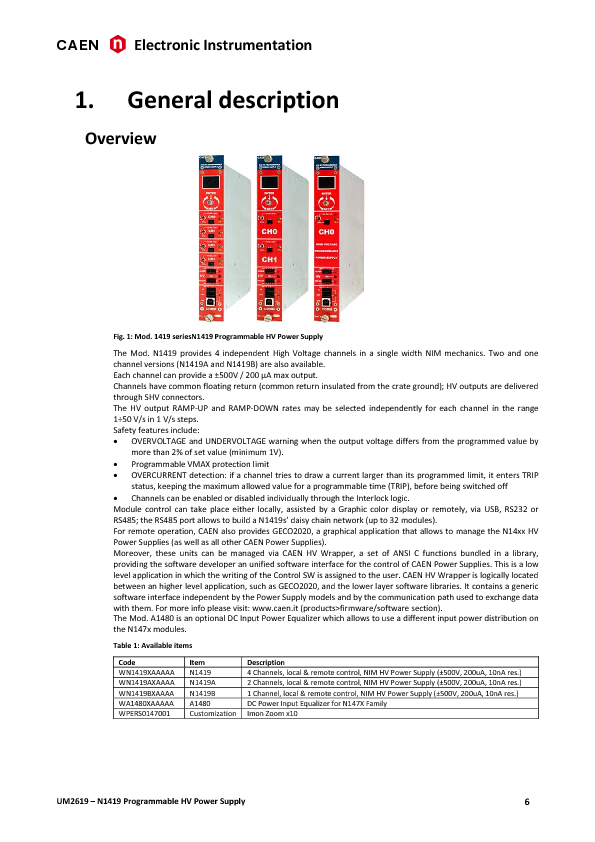
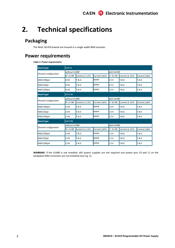
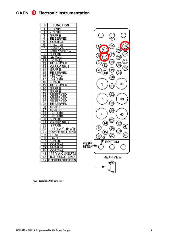
|
| Attachment 2: 30.png
|
|
|
73
|
Mon Apr 27 01:48:59 2015 |
JA, LHB, TD, VP, AE & CG | Monday 27 April 2015 |
DSSSD #1 +100V, +3.8uA
DSSSD #2 +100V, +5.5uA

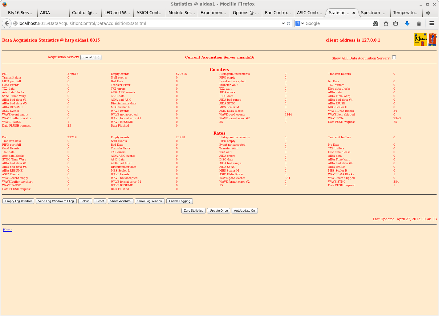
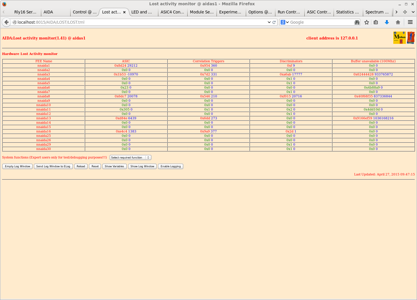
09.48 nnaida16 stalled at DAQ GO
      see attachments 1 & 2 for statistics & lost activity monitors

1830: Current FEE configuration (looking downstream):

                                   |          |           |           |
                                   |     x    |nnaida25+26|     x     |
                                   |          |           |           |
                                   |     x    |nnaida17+18|     x     |
                                   |          |           |           |
                                   |     x    |nnaida9+10 |     x     |
                                   |          |           |           |
                                   |     x    | nnaida1+2 |     x     |


 |nnaida |nnaida |nniada |nnaida |                                      |nnaida |nnaida |nniada |nnaida |
 |27+28  |19+20  |11+12  |3+4    |                                      |7+8    |15+16  |23+24  |31+32  |

                                   |          |           |           |
                                   |     x    | nnaida5+6 |nnaida13+14|
                                   |          |           |           |
                                   |     x    |     x     |     x     |
                                   |          |           |           |
                                   |     x    |nnaida21+22|     x     |
                                   |          |           |           |
                                   |     x    |nnaida29+30|     x     |


       Detector 1 (3131-11) is connected to nnaida 10, 11, 6, 16
       Detector 2 (3058-09) is connected to nnaida 2, 4, 14, 7
       Detector 3 (2977-20) is connected to nnaida 1, 3, 13, 8

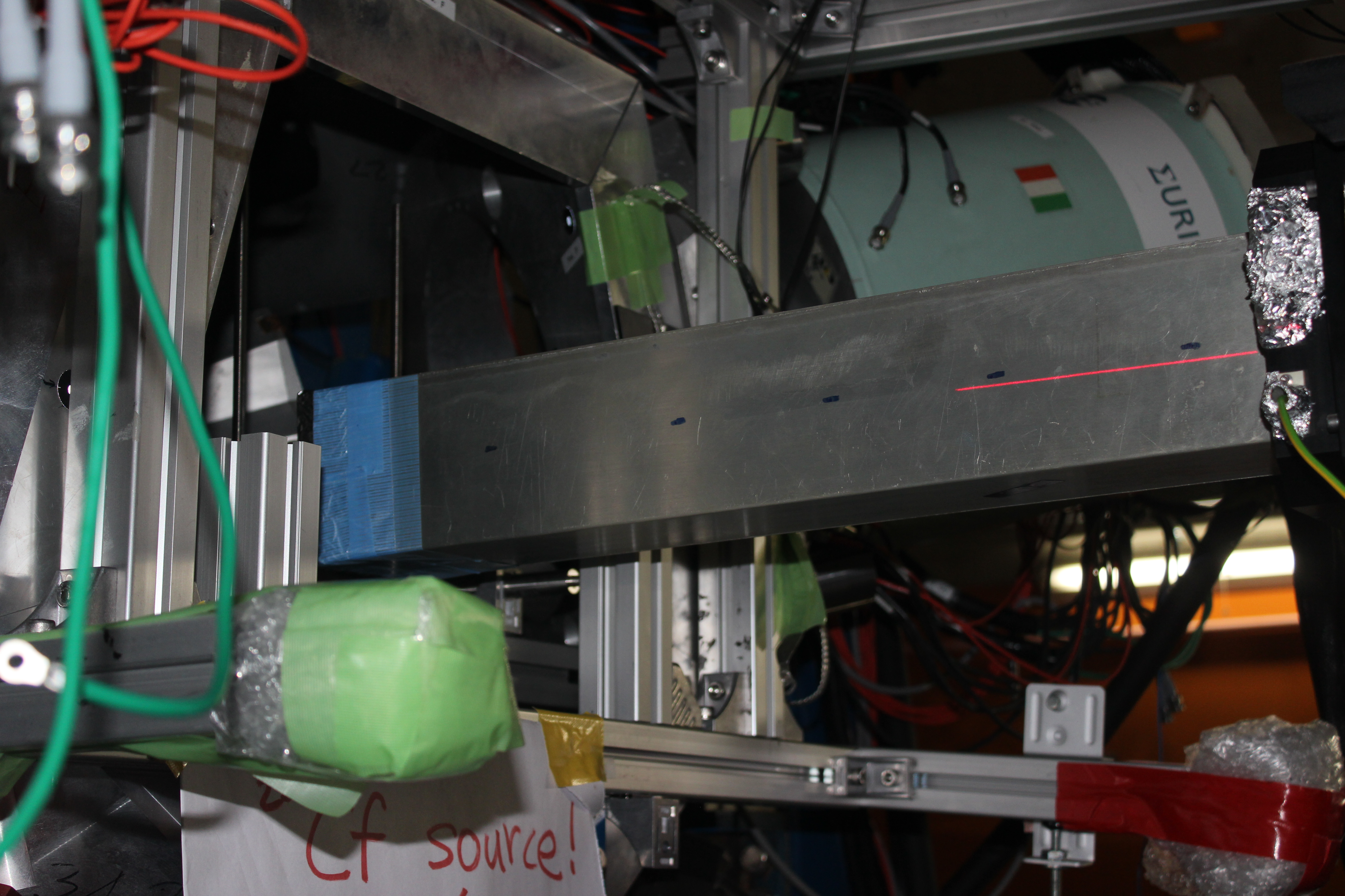
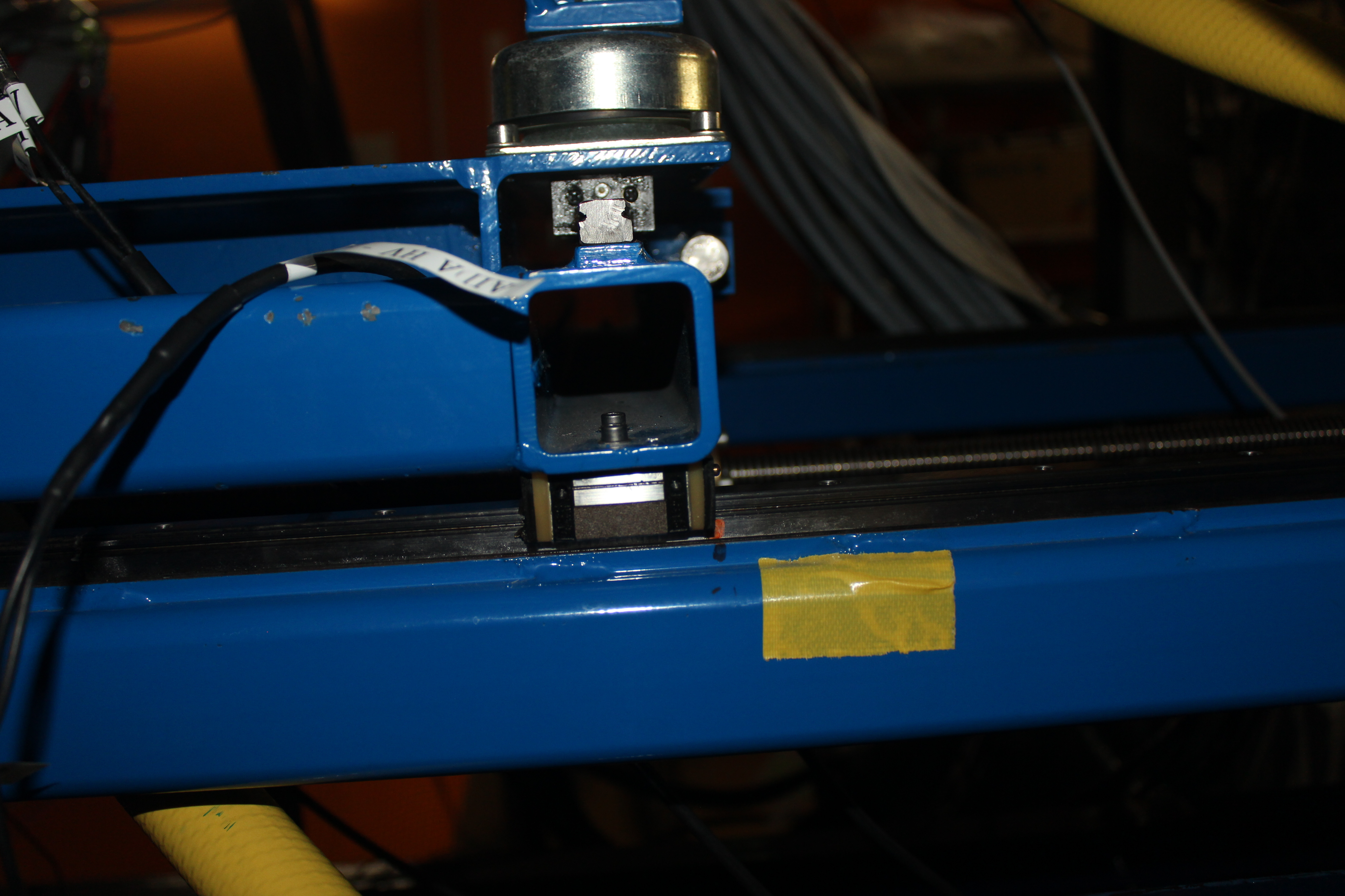
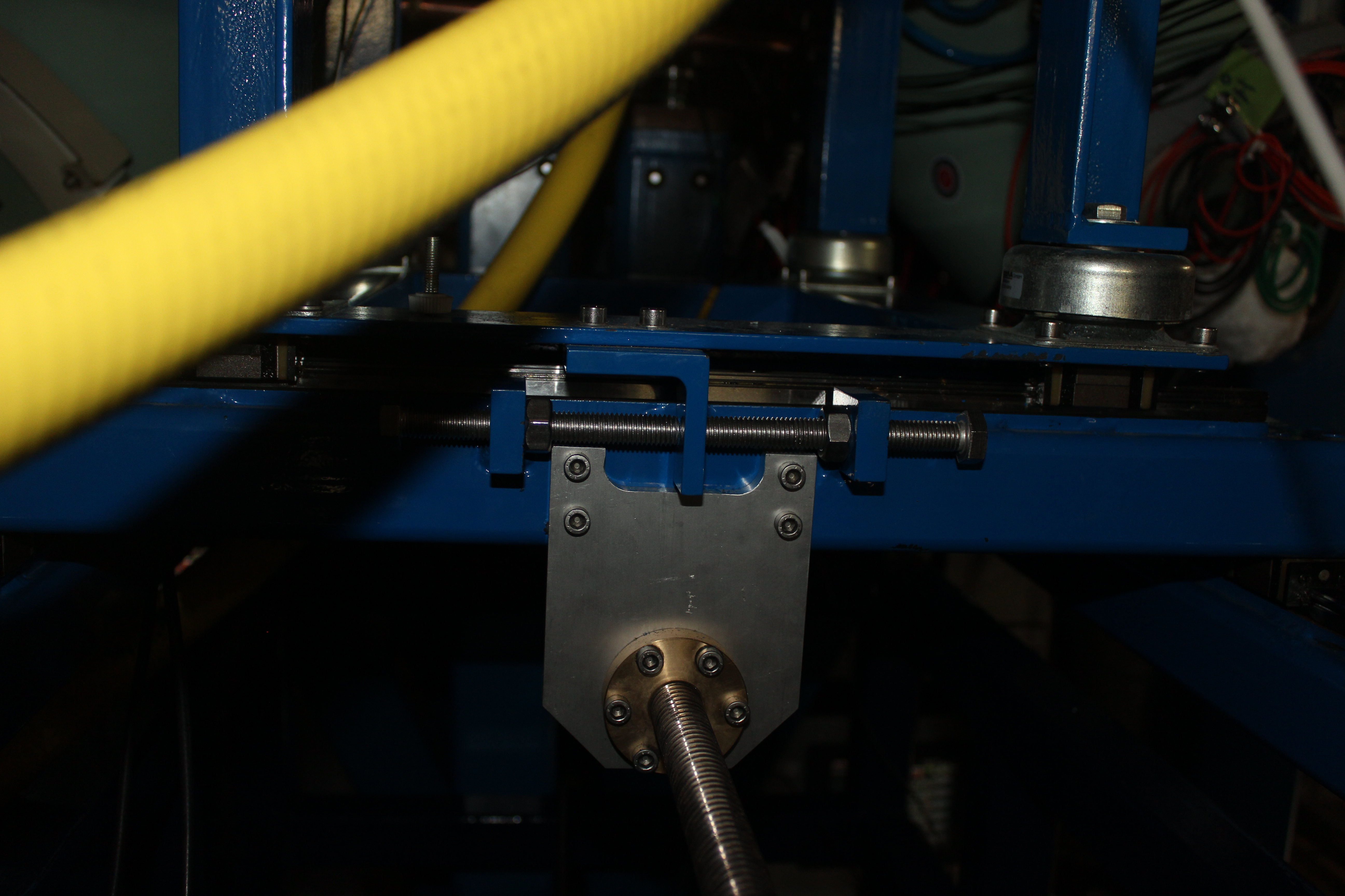
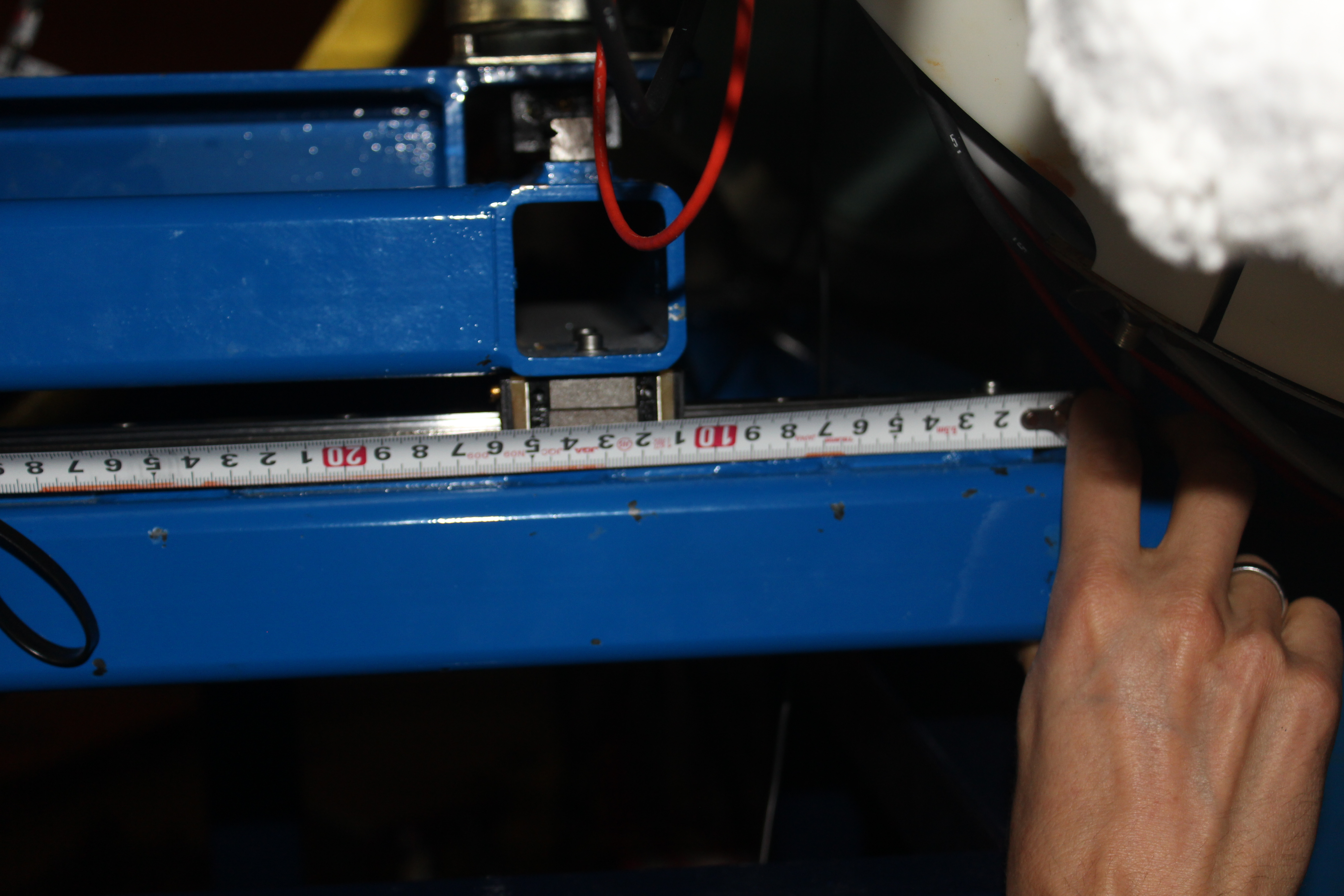
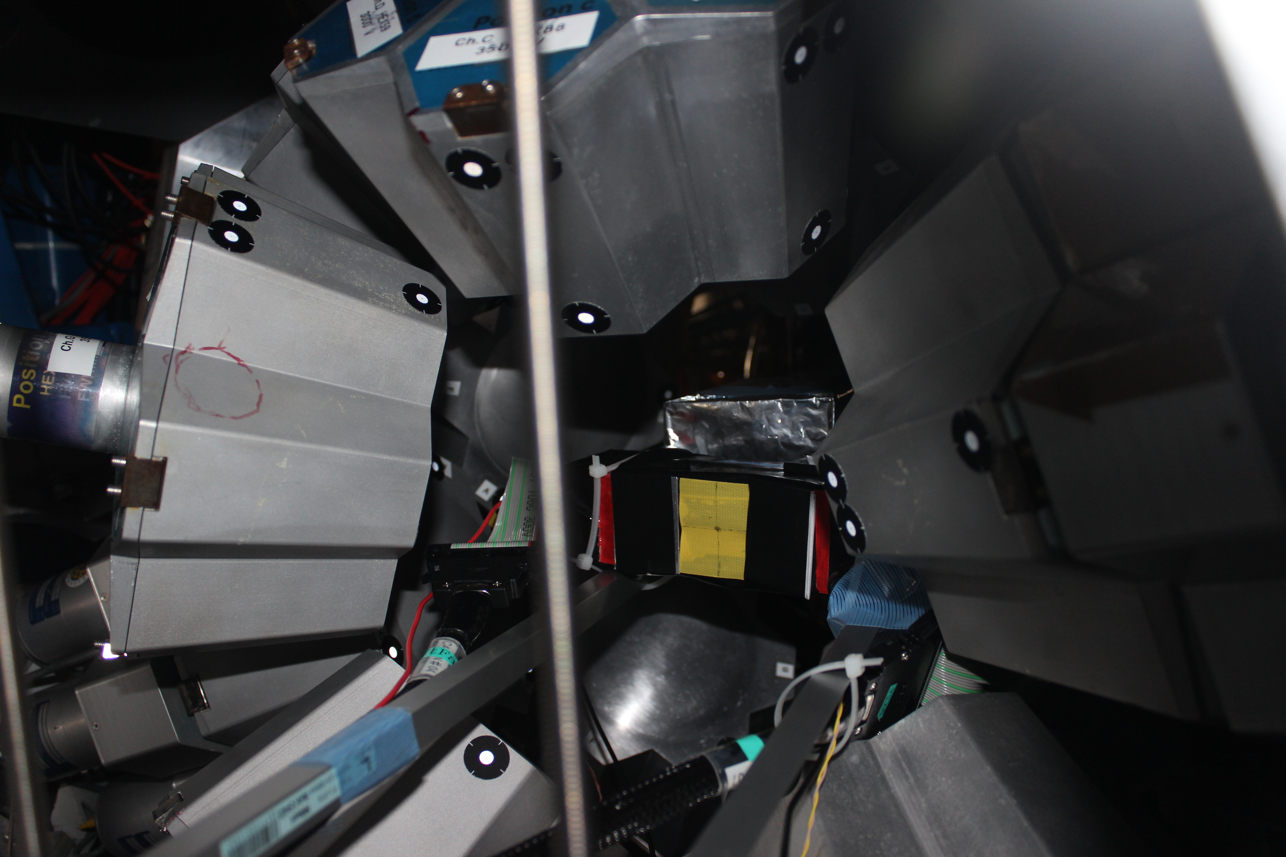
19.30 Check of AIDA alignment and positioning within EURICA
      See attachments 4-8

16.03 April 28  VP
     adding data sources (ie FEE64s) into the system and rules for TCP ports
  1) FEE needs to have an entry in the DHCP configuration  (/etc/dhcp/dhcp.conf)
    This assigns a host name (nnaidaxx) to the FEE based on ethernet MAC address and assigns an IP address
    10.1.1.xx   or  10.1.2.xx
     Also copy an existing file system in /MIDAS/XilinxLinux/ppc_4xx/rfs for nnaidaxx. This MUST be done as root
to preserve important file properties. (Use the existing tar file)
  2) The file /MIDAS/linux-ppc_4xx/startup/nnaidaxx  assigns xx as the AIDA Module Number and destination IP
port for created data.  In this example xx = 22.

    netstring TS_Server "myserver"
    netint TS_Port 11022
    netstring TS2_Server "myserver"
    netint TS2_Port 11122

    netint Aida_ModuleNum 22

    TS2_Server is currently not used

    So nnaidaxx  will send data to port 110xx in the Merger
  3)  Add nnaidaxx to the list of ACQSERVERS in /MIDAS/config/TclHttpd/aidas1/startup.tcl
  4)  The Merger configuration file is  /MIDAS/Merger/AIDA/GS_configuration
      If the highest Aida ModuleNum is xx then modify the links definition so you have
              links xx  ./link64 11001
      Note that xx may be greater than the actual number of FEE modules if there are gaps in your name scheme
      The highest enabled IP port will be (11001 + xx - 1)
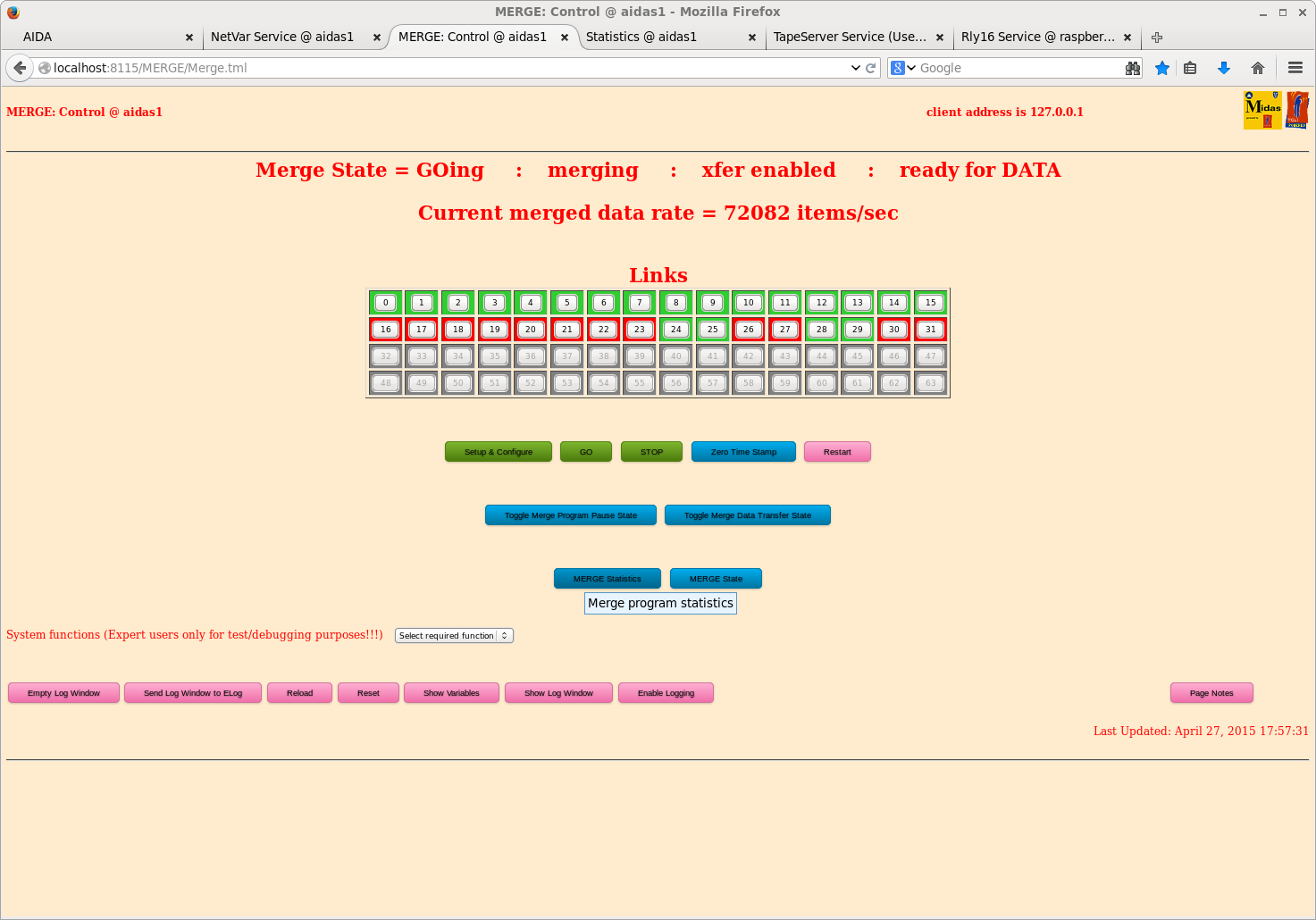
      You can enable/disable links to the Merge via the Merge GUI.
      Note: nnaidaxx appears to the Merge link table as link (xx-1).  So if you ask for 32 links they are
  0 => 31 in the Merge GUI table.
|
| Attachment 1: 20.png
|
|
| Attachment 2: 21.png
|
|
| Attachment 3: 22.png
|
|
| Attachment 4: IMG_2882.JPG
|
|
| Attachment 5: IMG_2889.JPG
|
|
| Attachment 6: IMG_2890.JPG
|
|
| Attachment 7: IMG_2891.JPG
|
|
| Attachment 8: IMG_2888.JPG
|
|
|
72
|
Sun Apr 26 02:28:59 2015 |
JA, LHB, TD, AE & CG | Sunday 26 April 2015 |
Upstream, 207Bi source

DSSSD #1  nnaida 6  & 9  (p+n), nnaida 11 & 16 (n+n)

DSSSD #2  nnaida 2  & 5  (p+n), nnaida 4  & 7  (n+n)

DSSSD #3  nnaida 1  & 14 (p+n), nnaida 3  & 8  (n+n)

N/C       nnaida 10 & 13 (p+n), nnaida 12 & 15 (n+n)

3x MSL type BB18(DS)-1000 DSSSDs connected via 12x flexible Kapton PCB cables to 8x adaptor PCBs


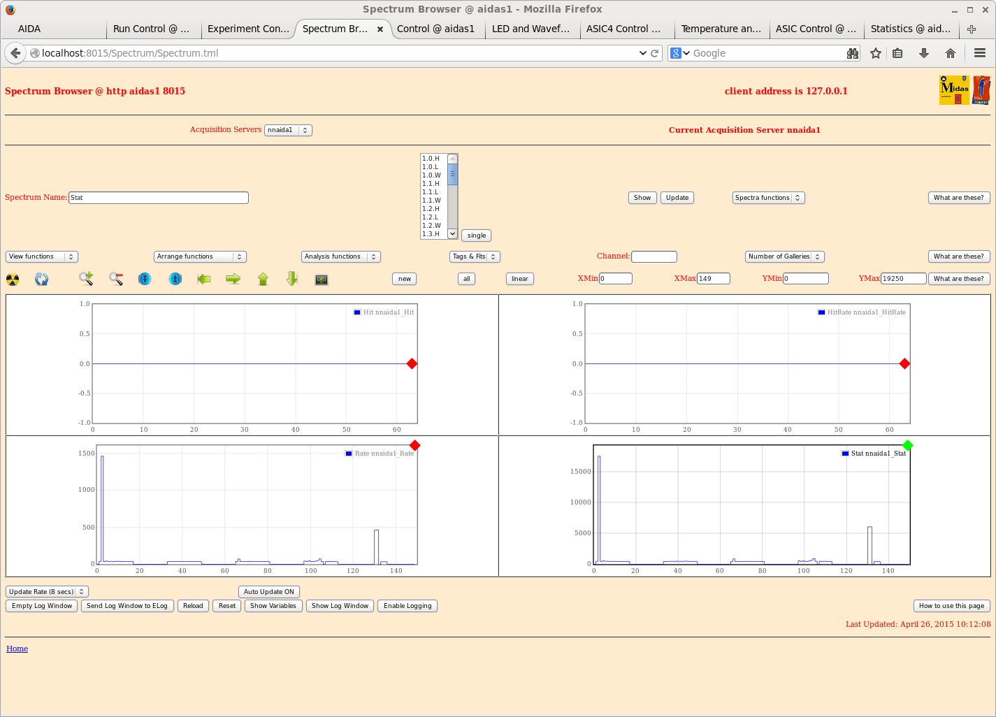
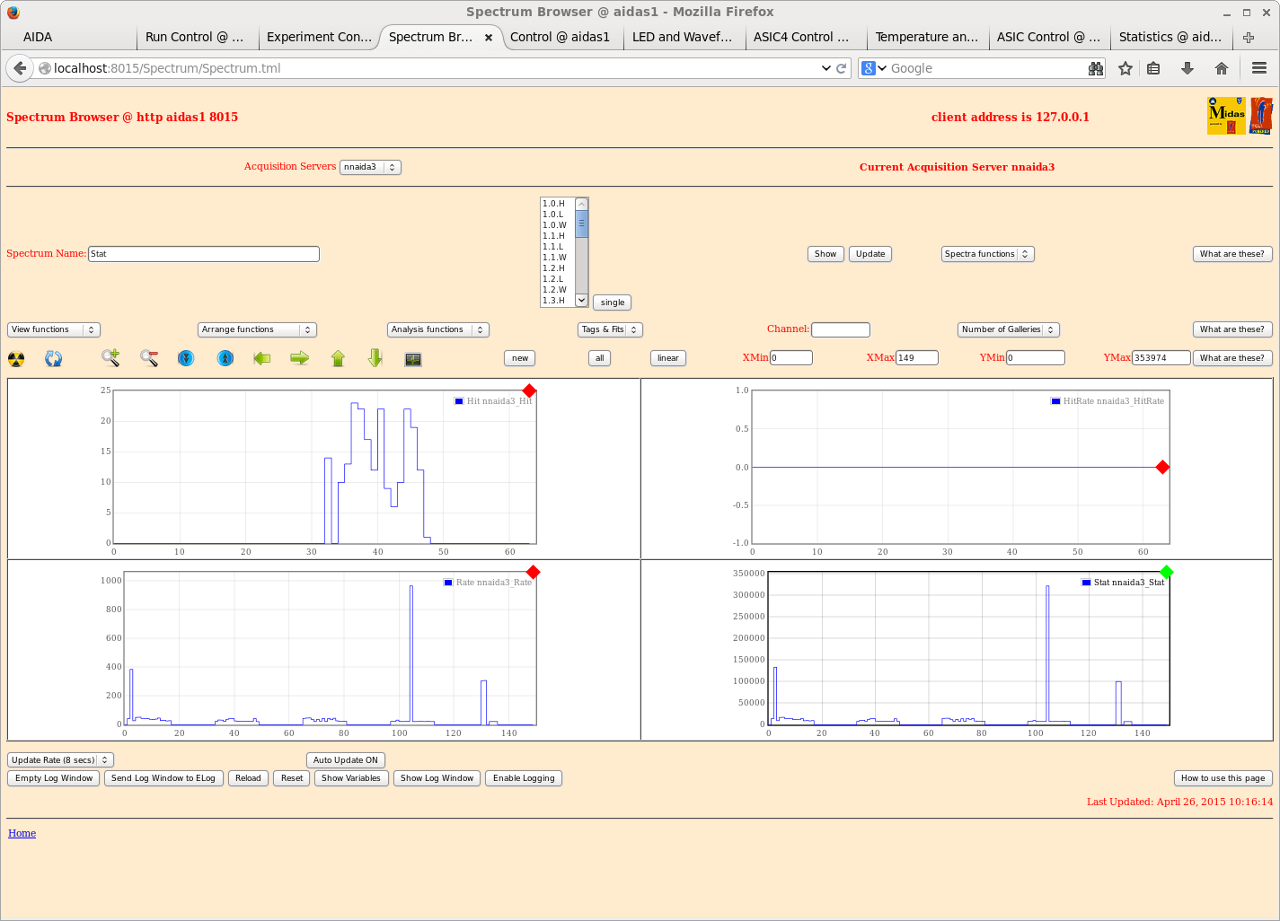
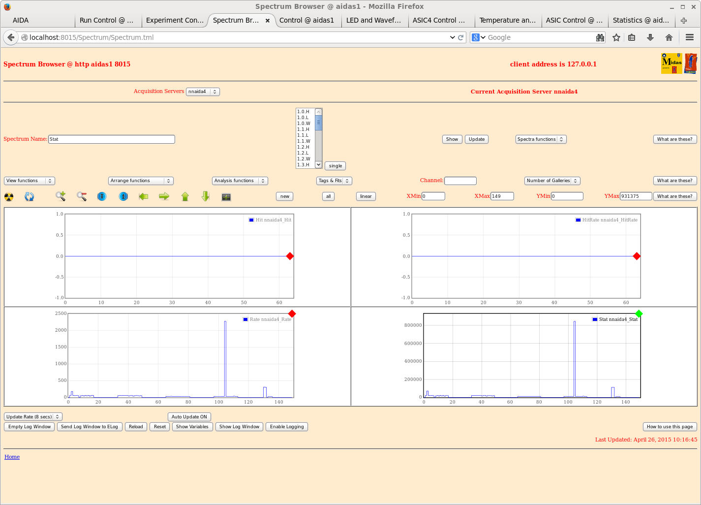
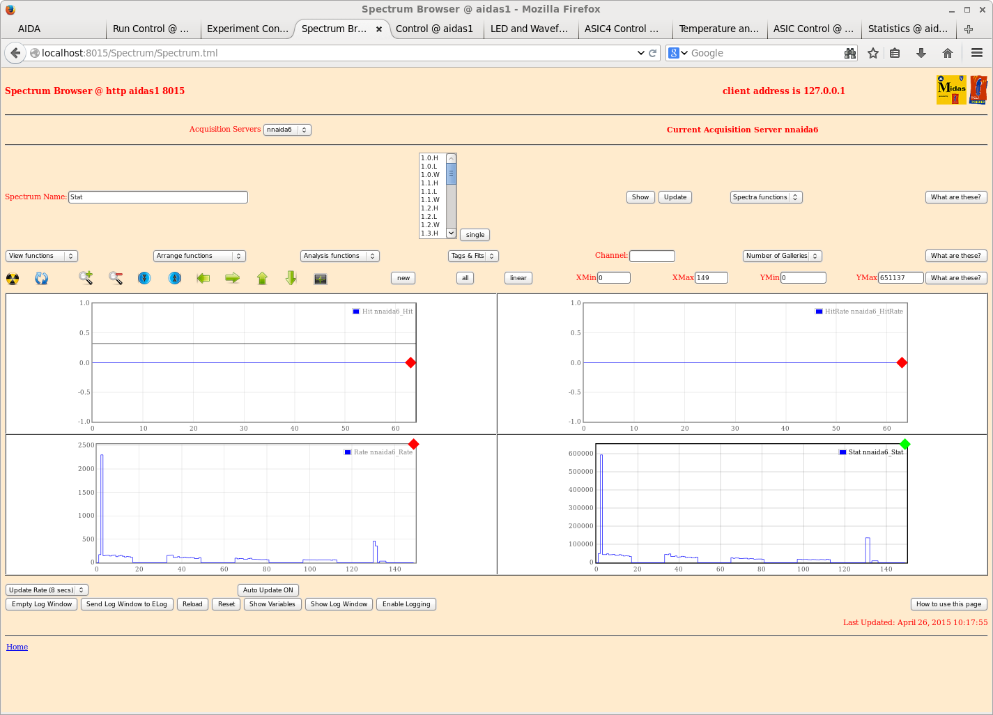
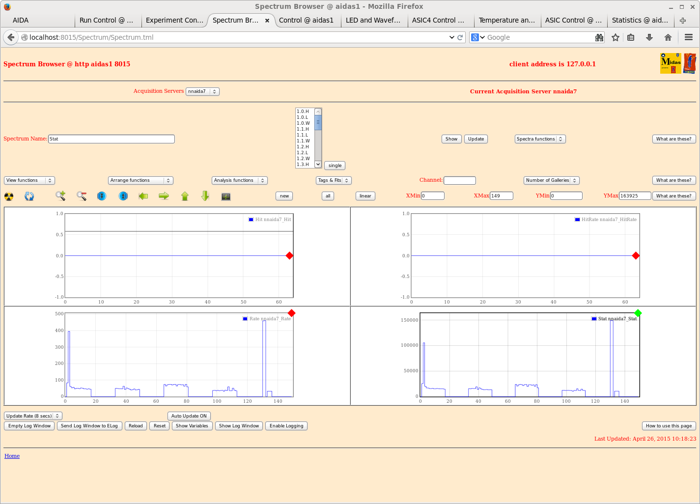
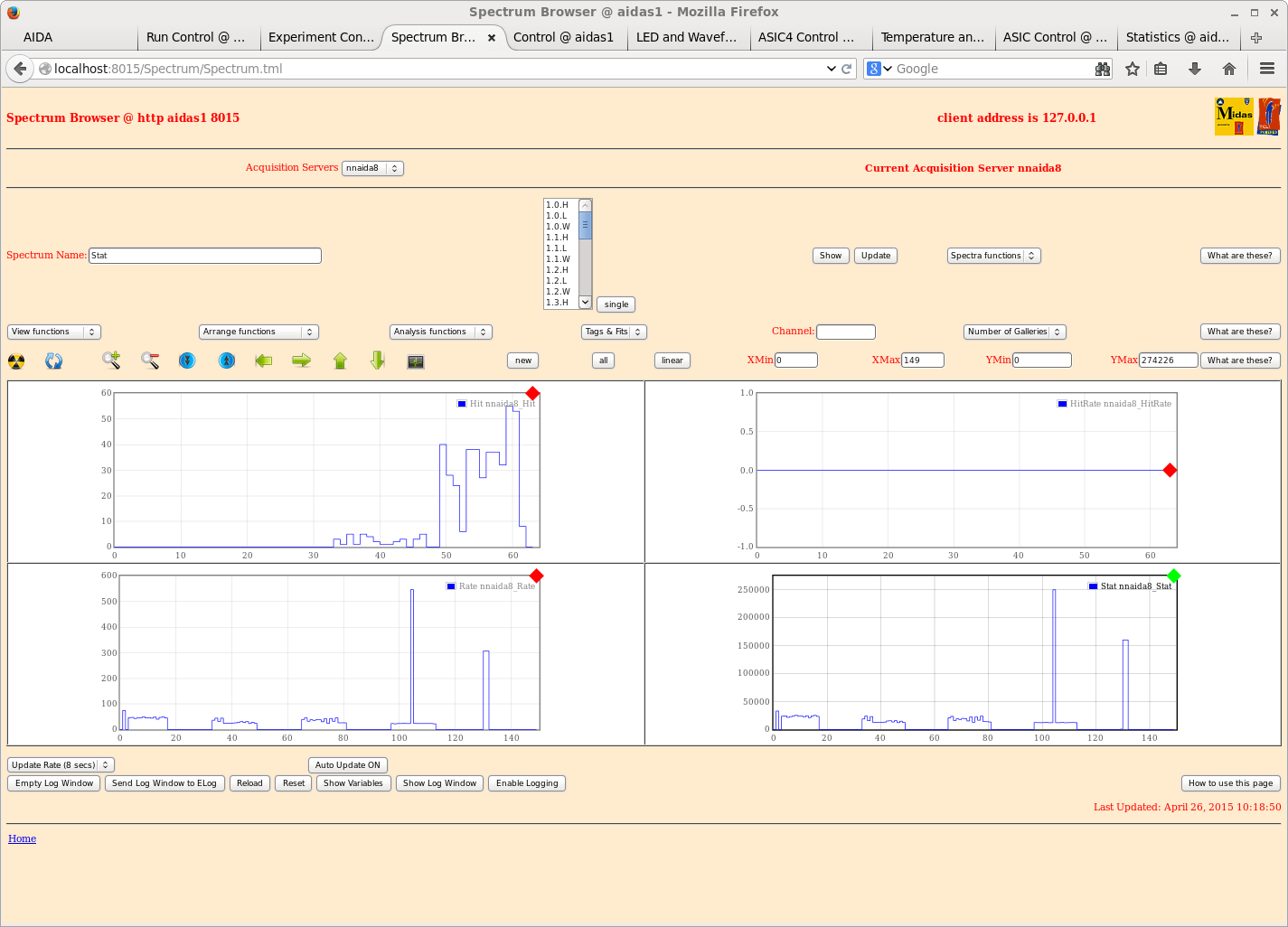
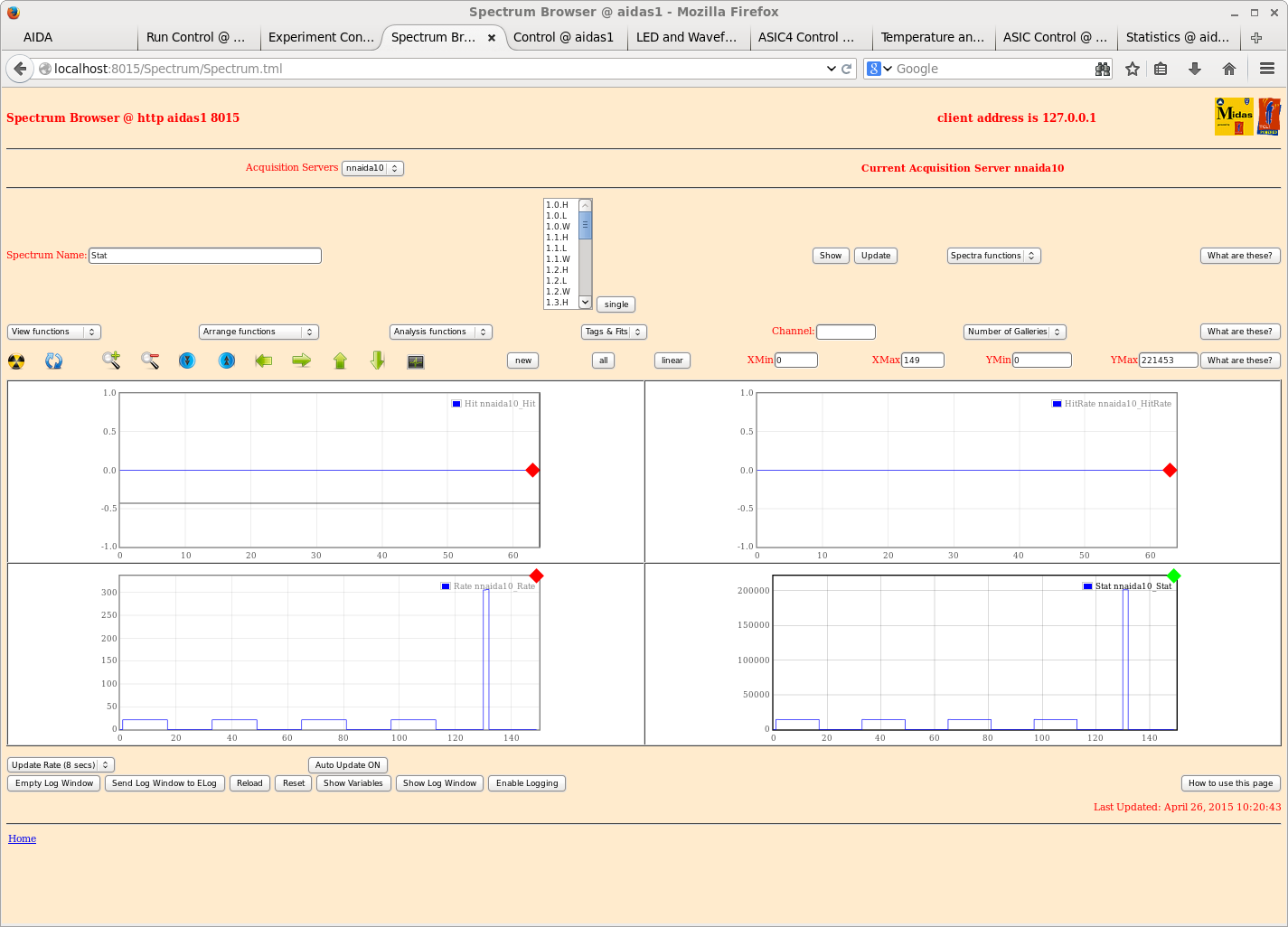
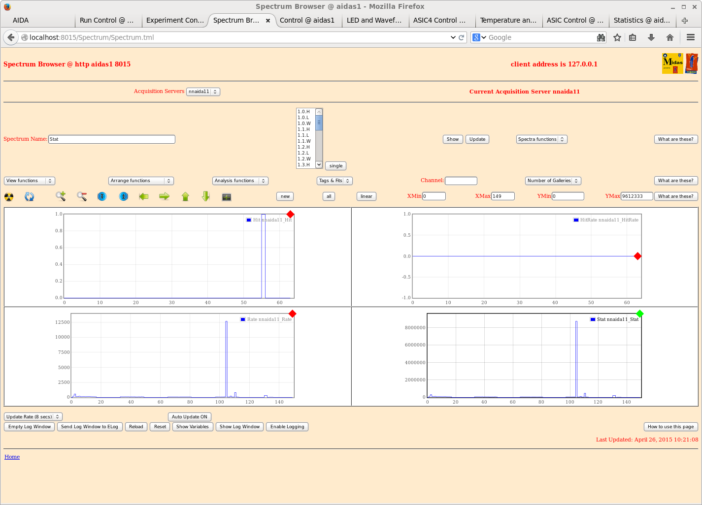
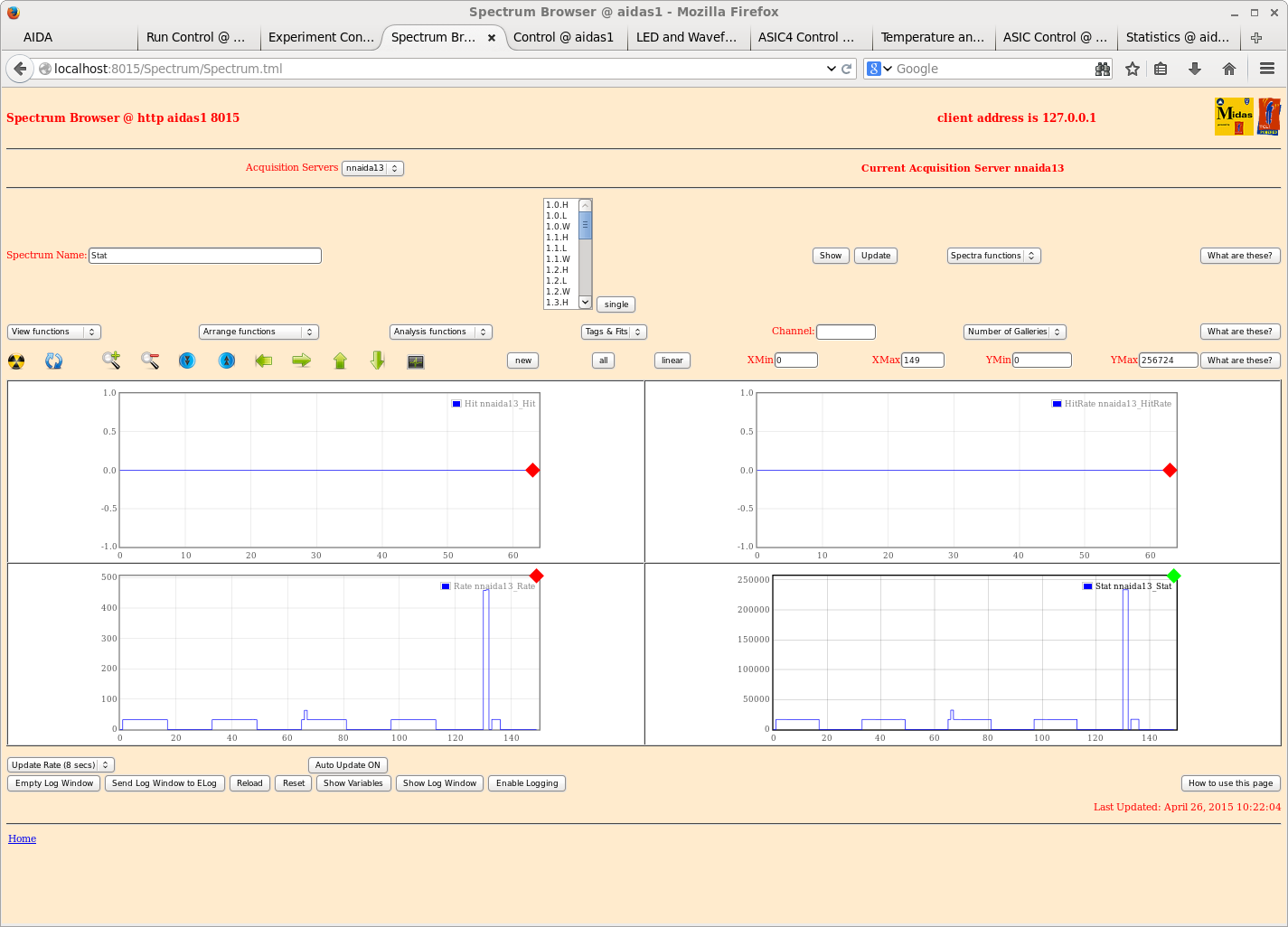
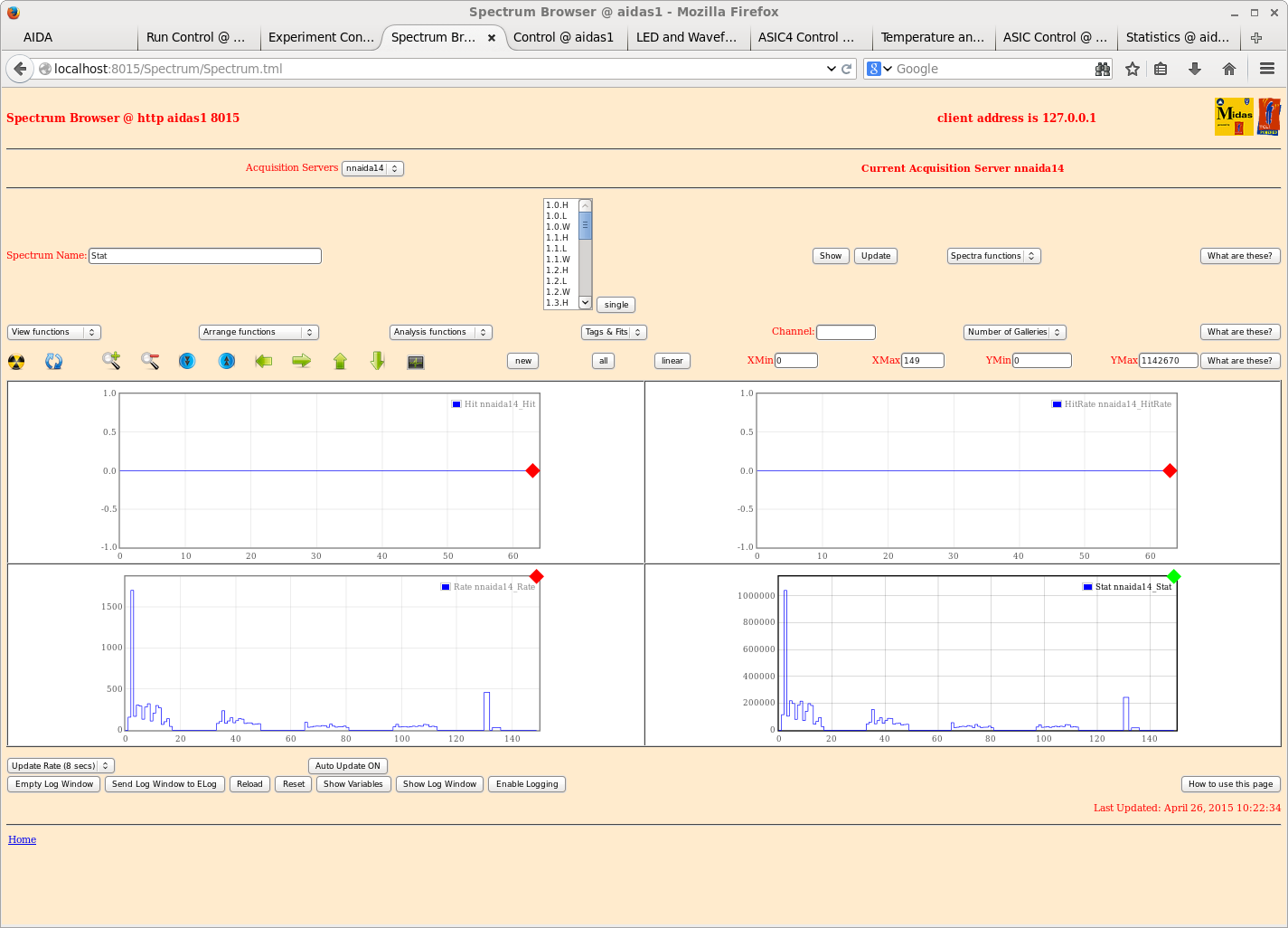
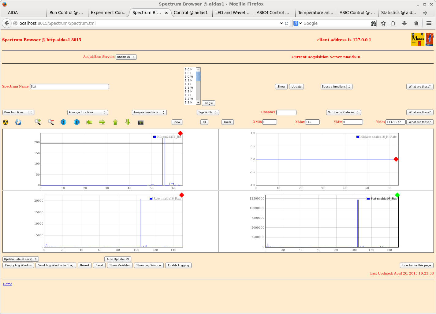
Hit patterns show attachments 1-16


Default ASIC parameters *except* slow comparator 0x10 -> 0x20

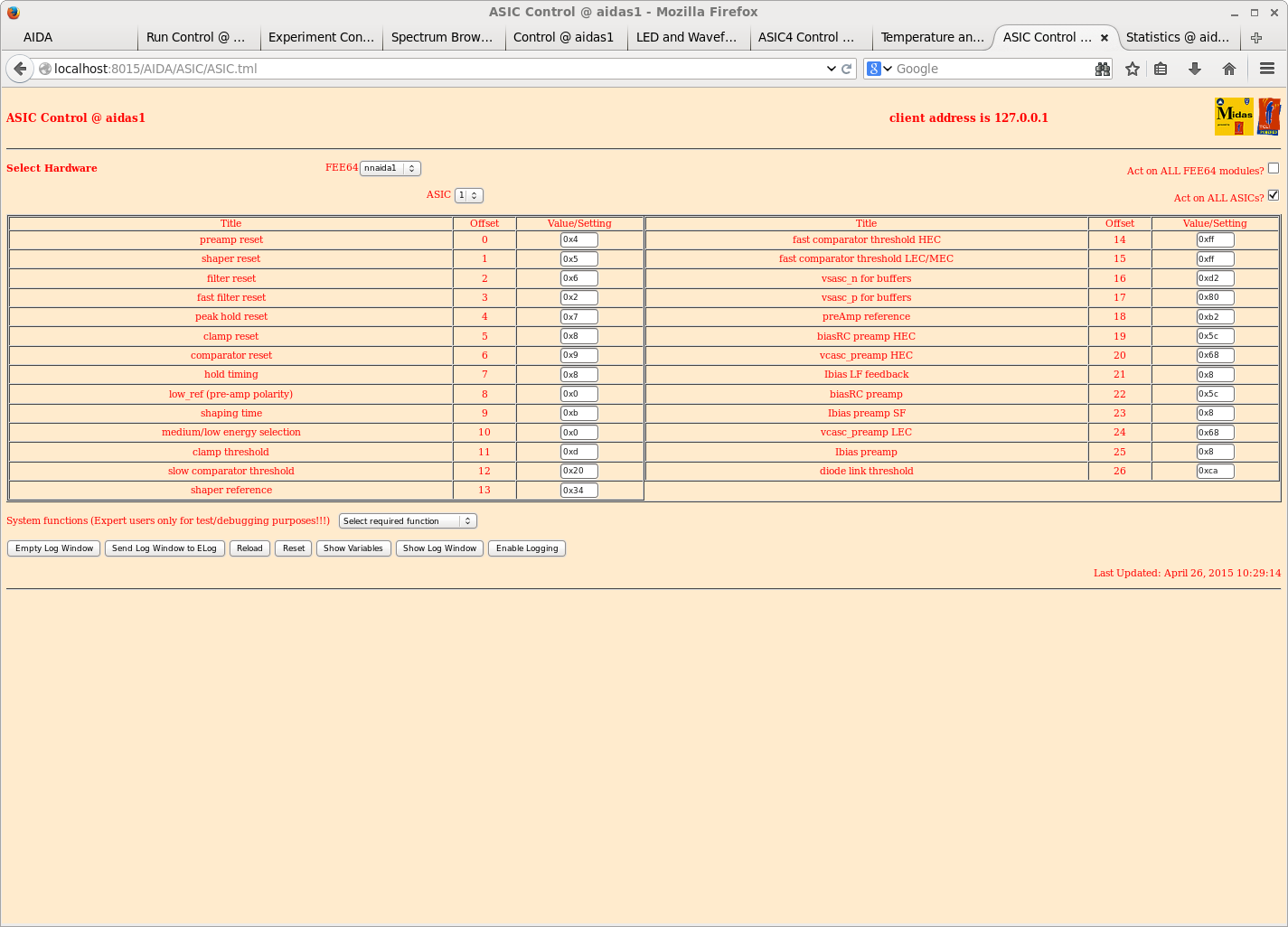
Example ASIC configuration attachment 17

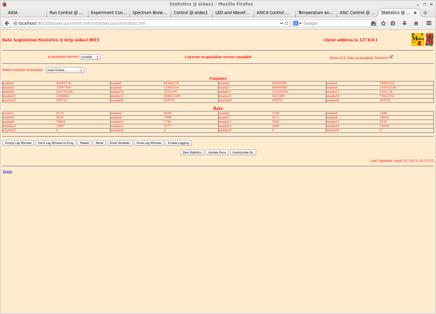
Example 'Good Events' statistics attachment 18


ASIC #1 waveforms of nnaida 1 - 16 enabled

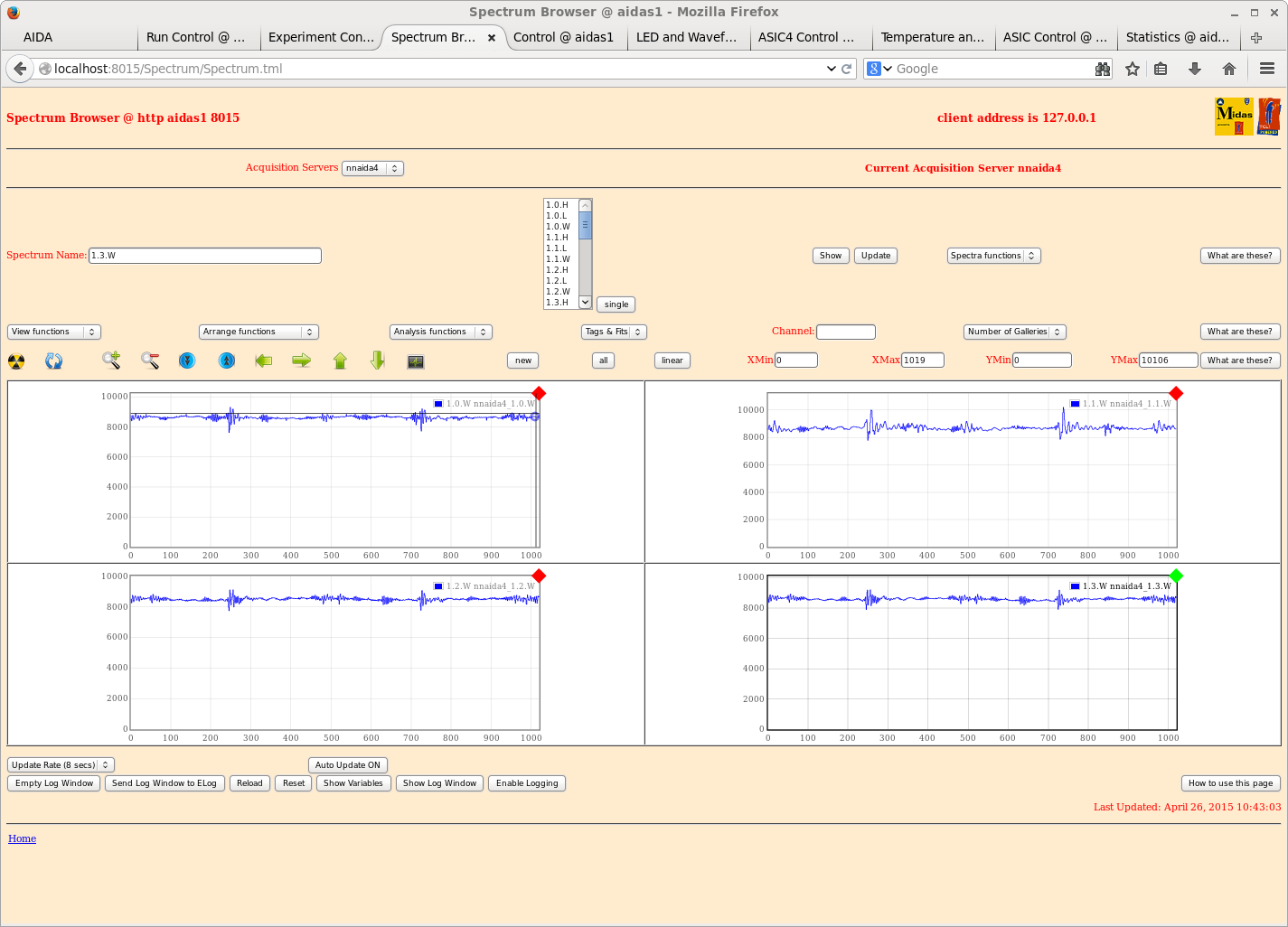
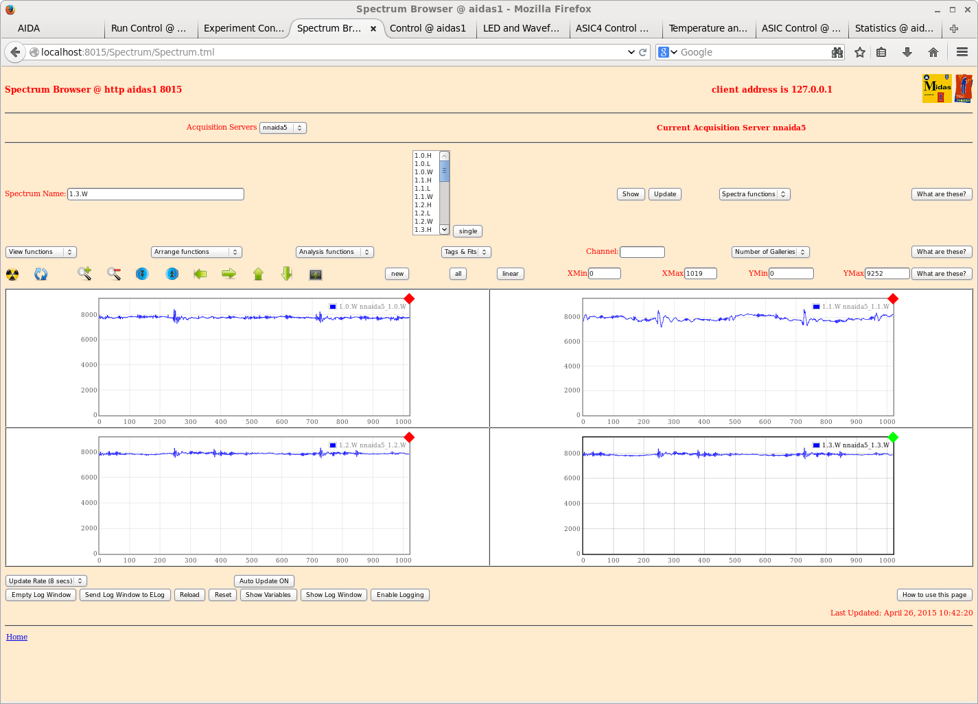
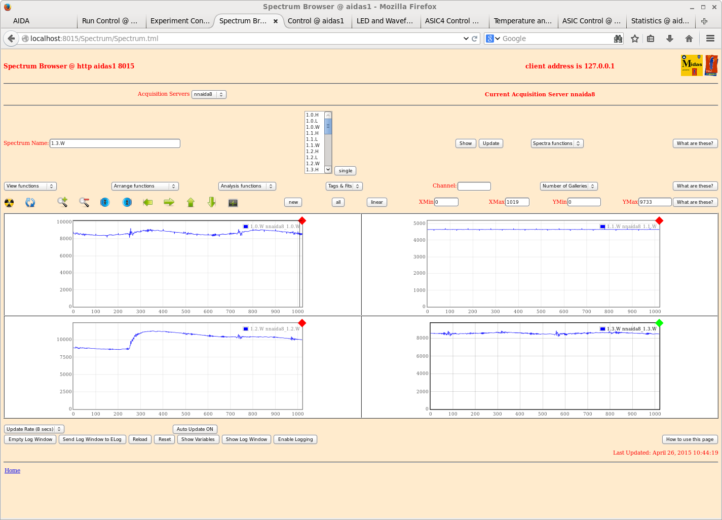
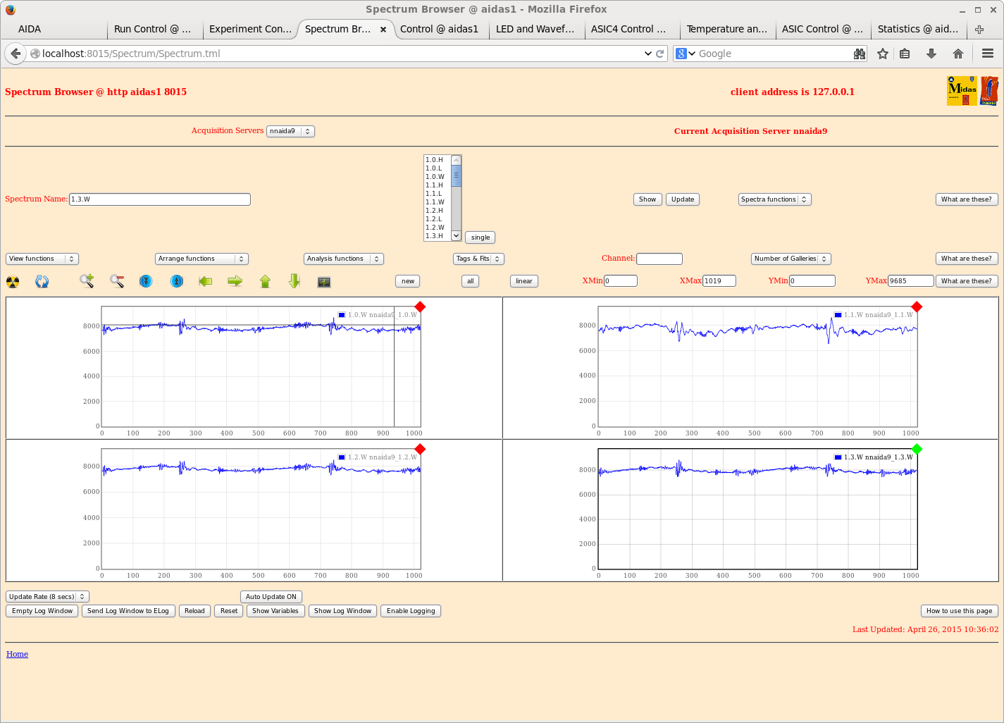
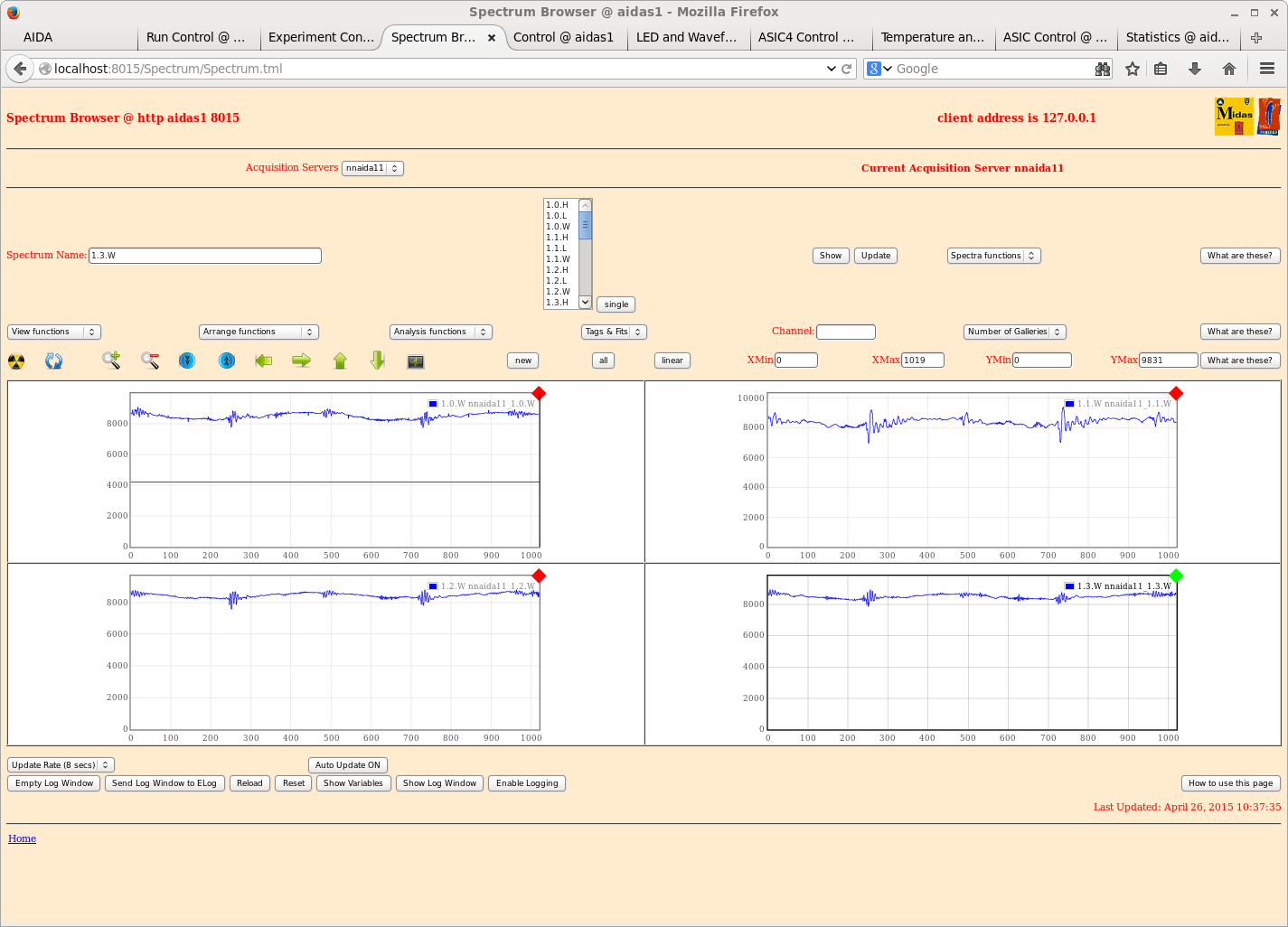
Example waveform for p+n and n+n strips of each DSSSD attachments 19-24


Parameters saved to: /MIDAS/DB/EXPERIMENTS/AIDA/2015Apr26-10.56.40


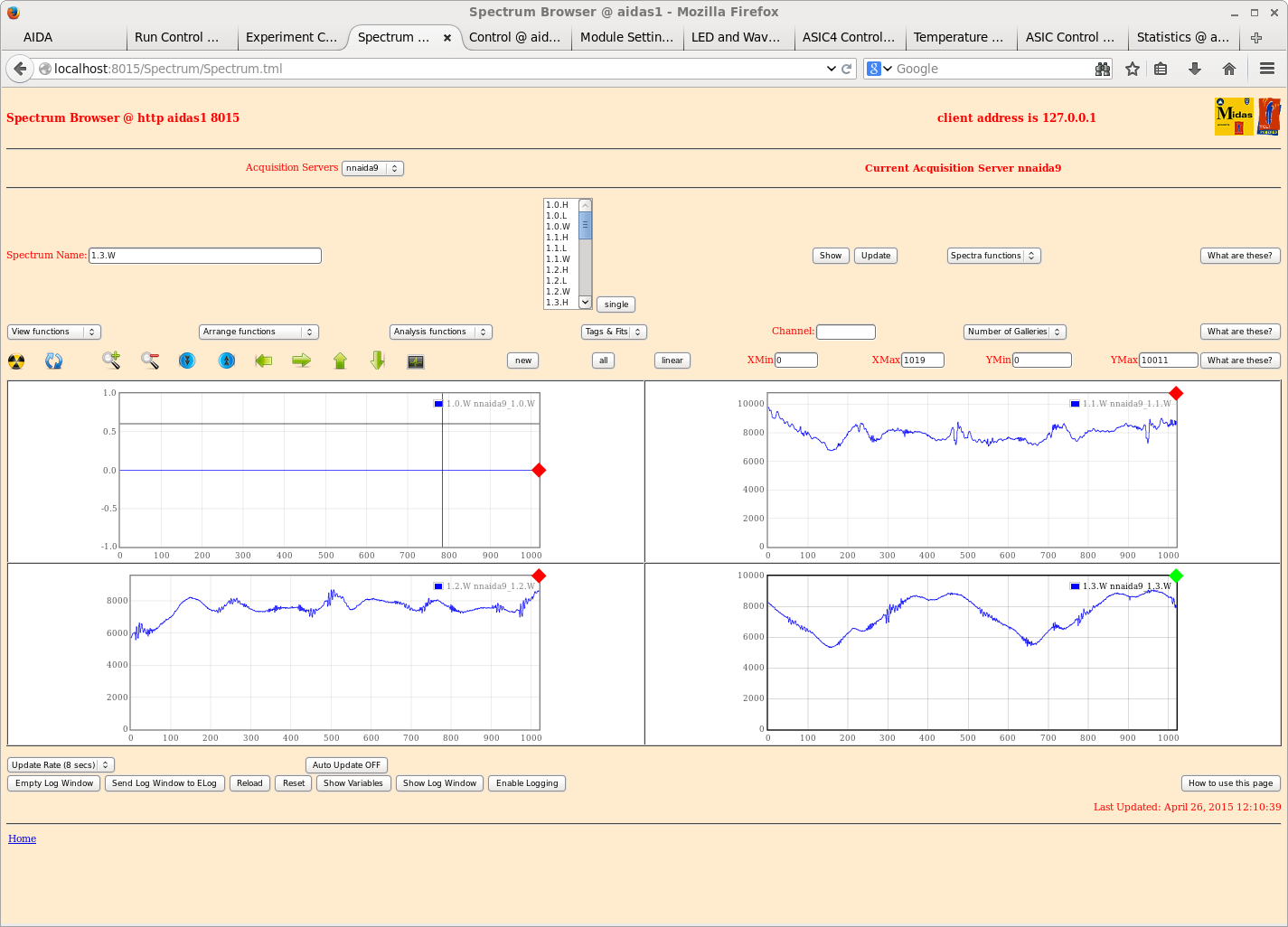
12.10 Removing bias gnd jumper from p+n adaptor PCBs increases amplitude of ~100kHz RFI/EMI
      (attachment 25)

15.20 Reduce DSSSD configuration to 1x DSSSD using 4x adaptor PCBs + heavy duty copper braid
      DSSSD #2 nnaida 2 & 14 (p+n), nnaida 4 & 7 (n+n)

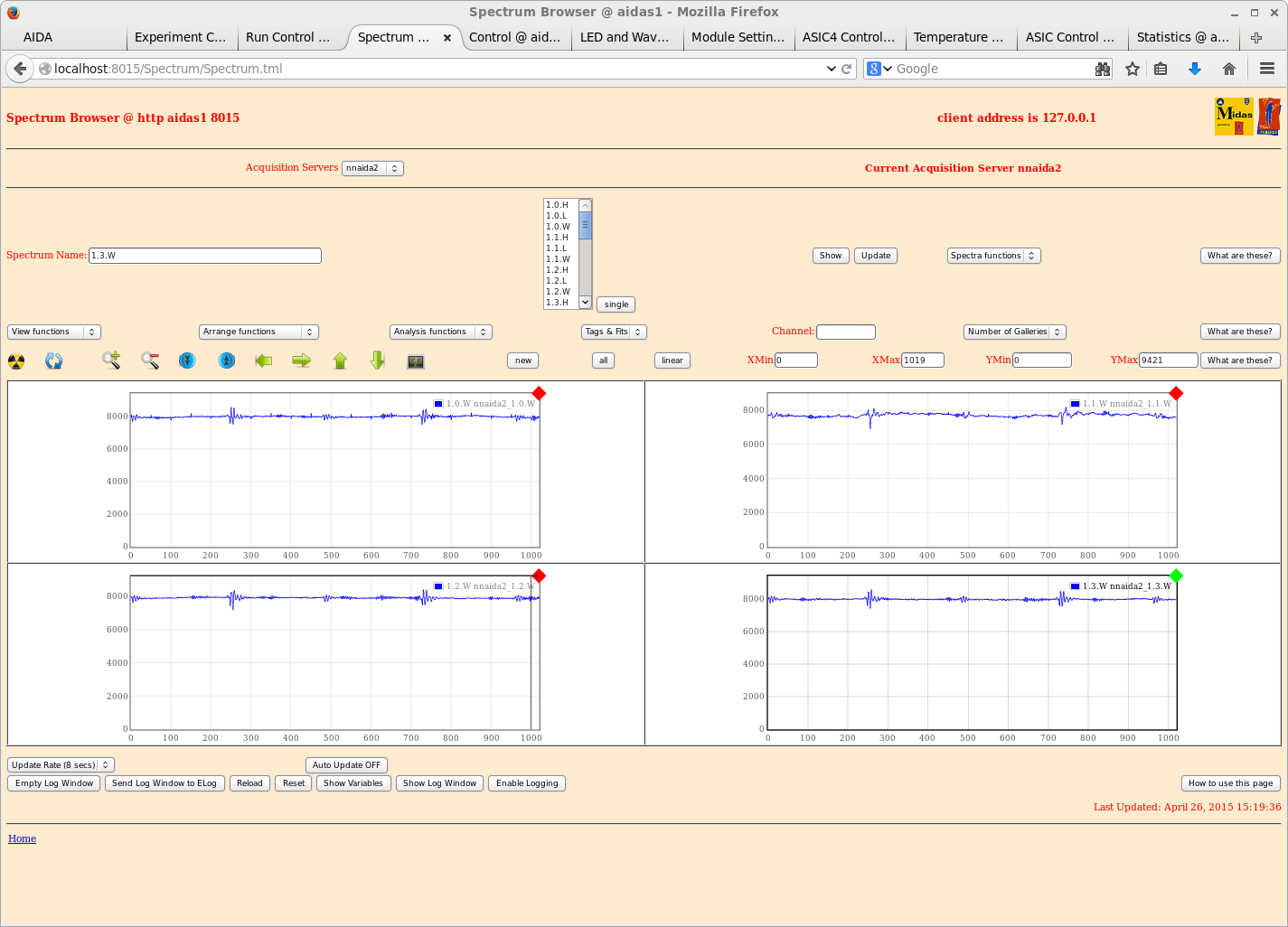
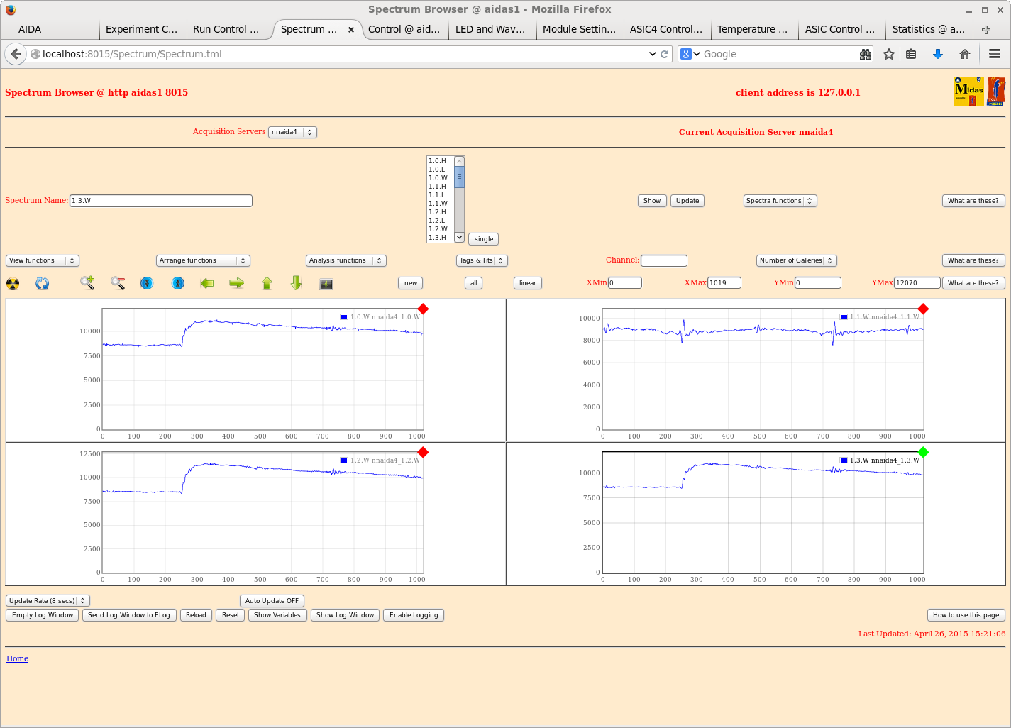
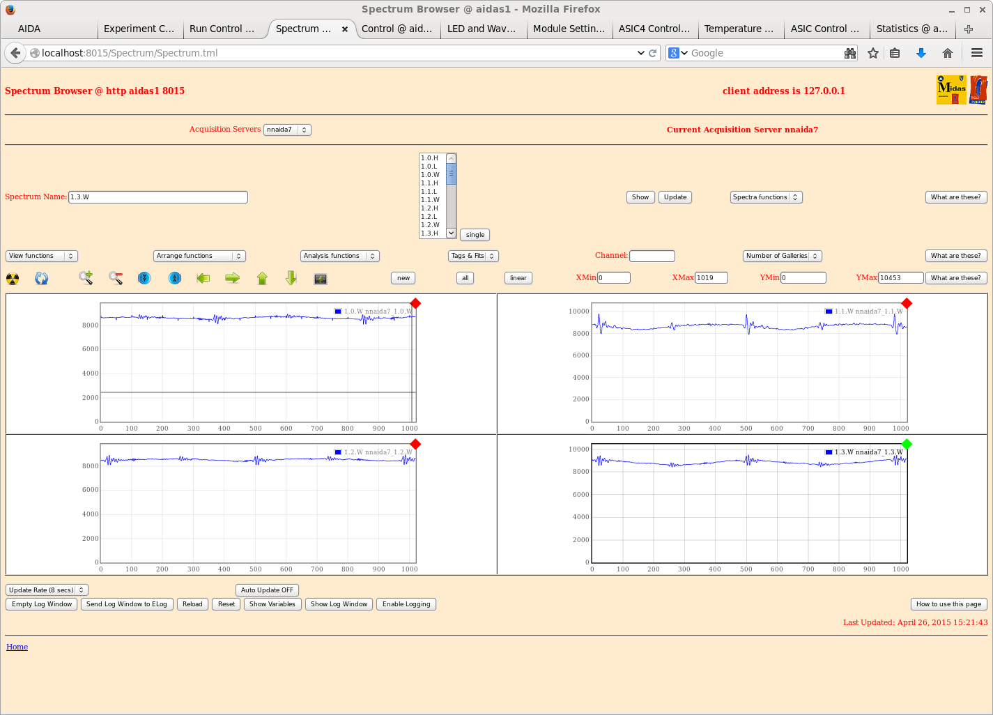
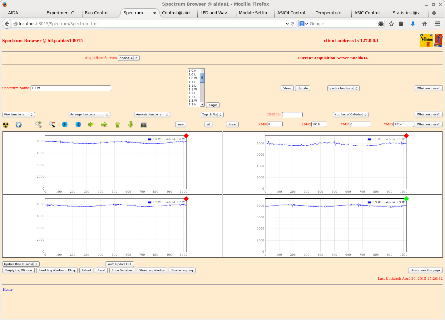
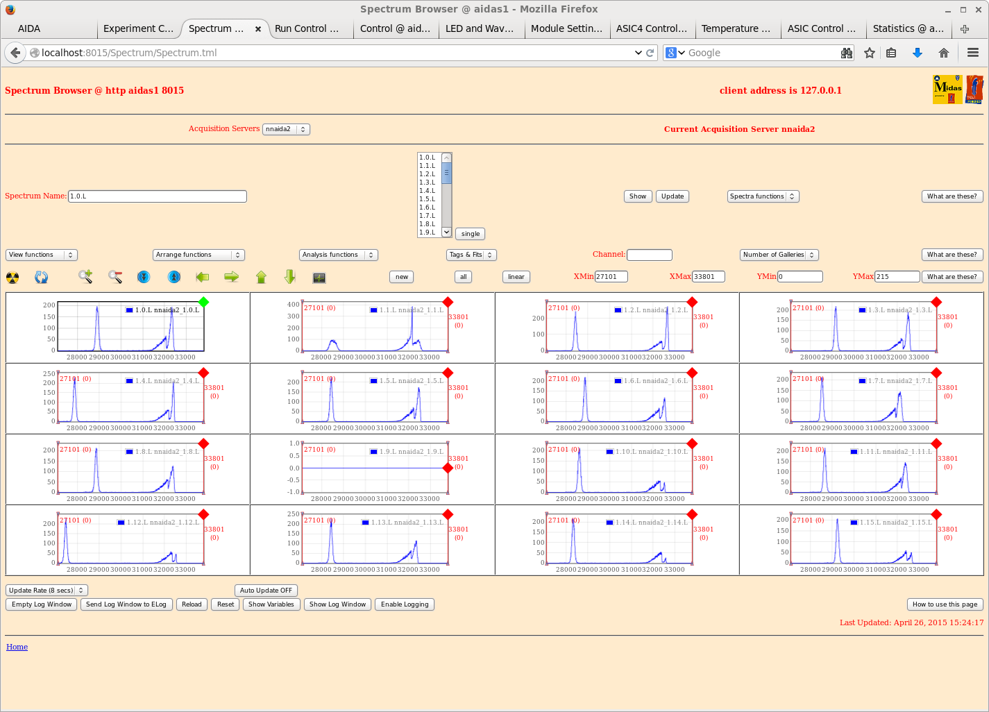
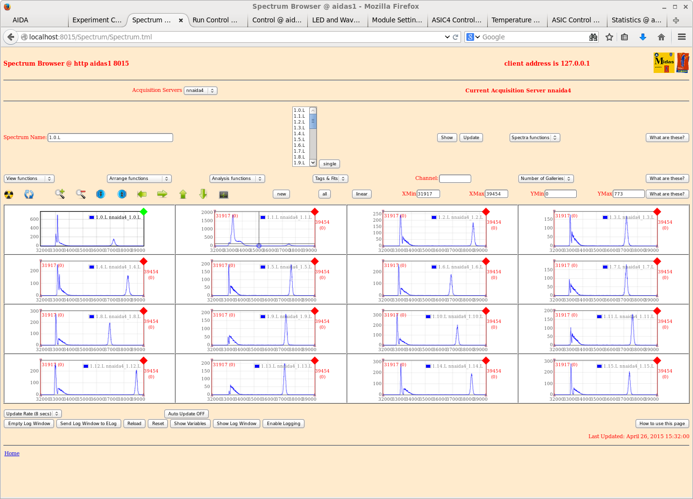
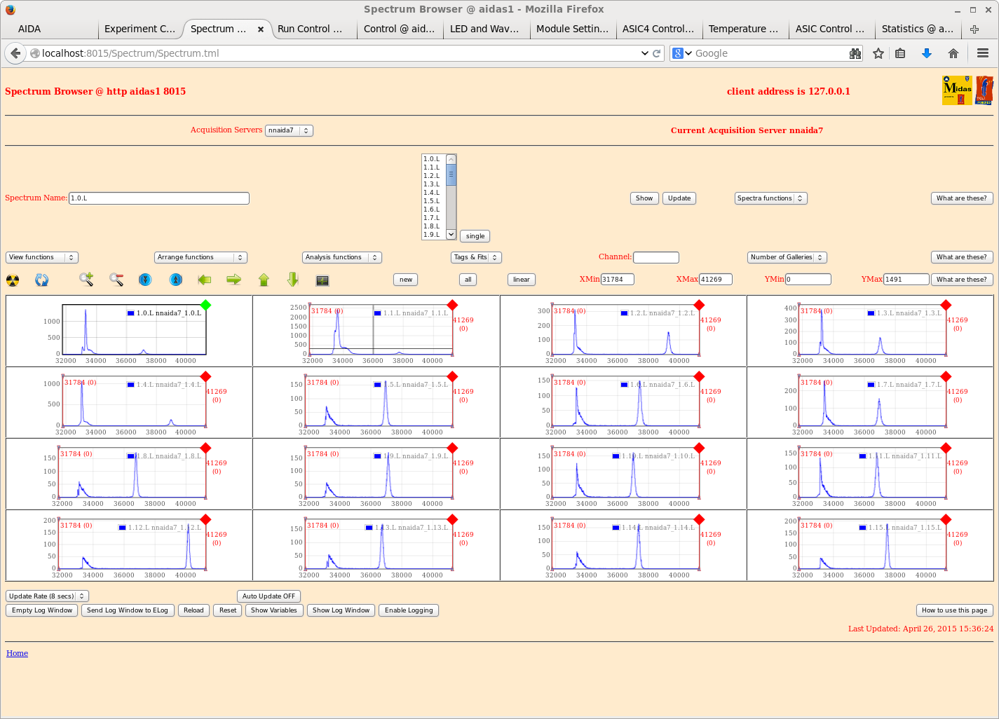
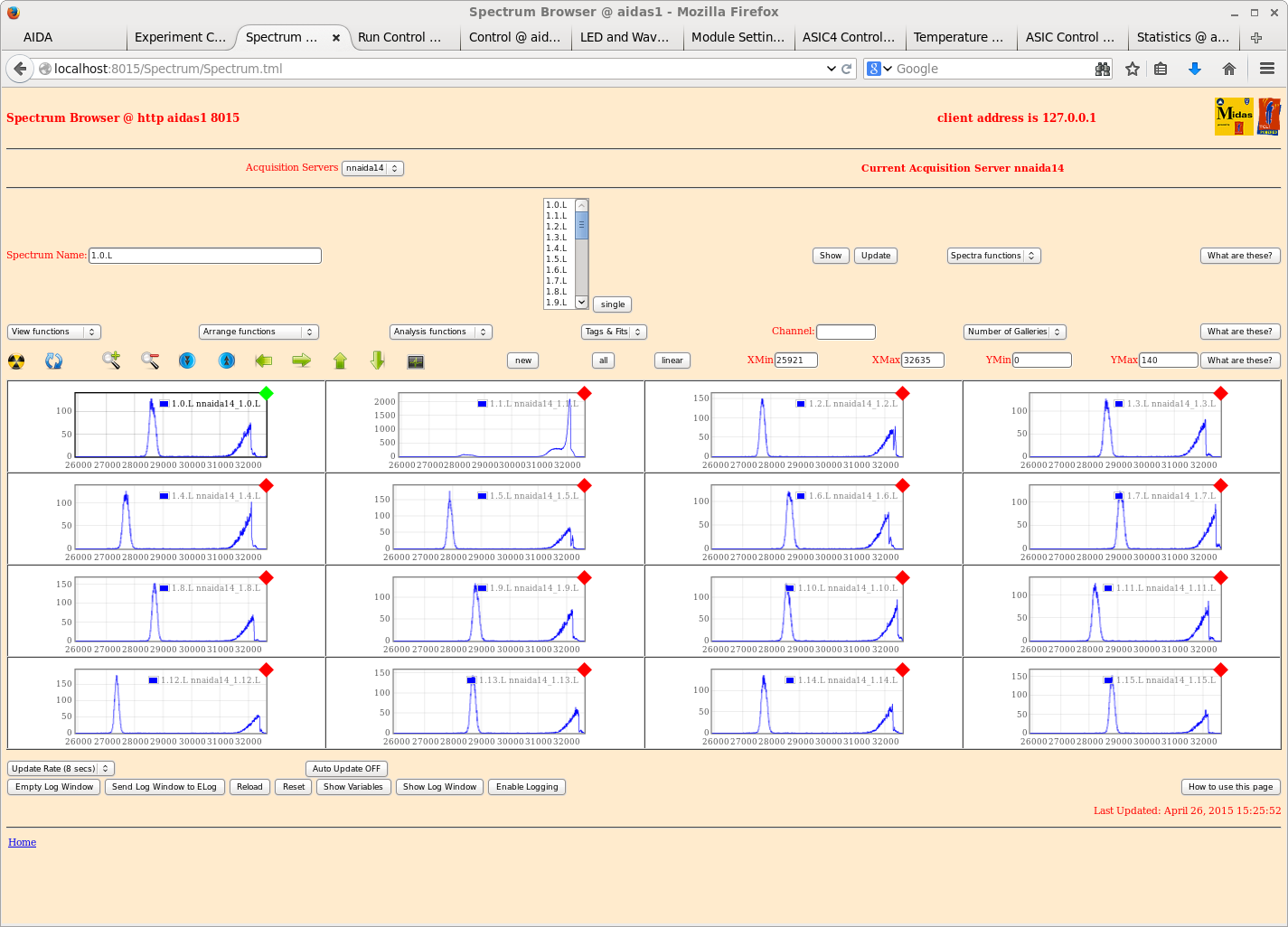
      attachments 26-33 show example preamp traces and ASIC#1 spectra

      similar stability/performance to previous tests with a single DSSSD, typical pulser
      peak widths ~130-200 ch FWHM

      AIDA snout drain wire - no obvious difference if connected, or not (as before)

15.40 DSSSD configuration 2x DSSSD using 8x adaptor PCBs
      DSSSD #2 nnaida 2 & 14 (p+n), nnaida 4 & 7 (n+n) + heavy duty copper braid
      DSSSD #1 nnaida 6 & 10 (p+n), nnaida 11 & 16 (n+n) + black jumper cables from above adaptor PCBs
      to these adaptor PCBs
      Detector bias from N1419 and N1419B, i.e. separate NIM modules => separate floating grounds
      similar or improved performance to 1x DSSSD test, typical pulser peak widths ~115-250 ch FWHM

16.15 CG smartphone camera pictures of front end config

16.30 data to disk - file /Tapedata/May2015/R3_0.gz (BNC Pb-4 25Hz + 207Bi source)

17.30 Detector bias from N1419, i.e. both detector biases from same NIM module => same floating ground
      for both DSSSDs

      Similar performance to case above (separate NIM modules)

17.46 data to disk - file /Tapedata/May2015/R4_0.gz (BNC Pb-4 25Hz + 207Bi source) |
| Attachment 1: 1.png
|
|
| Attachment 2: 2.png
|

|
| Attachment 3: 3.png
|
|
| Attachment 4: 4.png
|
|
| Attachment 5: 5.png
|

|
| Attachment 6: 6.png
|
|
| Attachment 7: 7.png
|
|
| Attachment 8: 8.png
|
|
| Attachment 9: 9.png
|

|
| Attachment 10: 10.png
|
|
| Attachment 11: 11.png
|
|
| Attachment 12: 12.png
|

|
| Attachment 13: 13.png
|
|
| Attachment 14: 14.png
|
|
| Attachment 15: 15.png
|

|
| Attachment 16: 16.png
|
|
| Attachment 17: 17.png
|
|
| Attachment 18: 18.png
|
|
| Attachment 19: 1w.png
|

|
| Attachment 20: 4w.png
|
|
| Attachment 21: 5w.png
|
|
| Attachment 22: 8w.png
|
|
| Attachment 23: 9w.png
|
|
| Attachment 24: 11w.png
|
|
| Attachment 25: 9w-bias-jumper.png
|
|
| Attachment 26: 2w-1.png
|
|
| Attachment 27: 4w-1.png
|
|
| Attachment 28: 7w-1.png
|
|
| Attachment 29: 14w-1.png
|
|
| Attachment 30: 2-1.png
|
|
| Attachment 31: 4-1.png
|
|
| Attachment 32: 7-1.png
|
|
| Attachment 33: 14-1.png
|
|
|
71
|
Sat Apr 25 03:56:44 2015 |
JA, LHB, TD, AE & CG | Saturday 25 April 2015 |
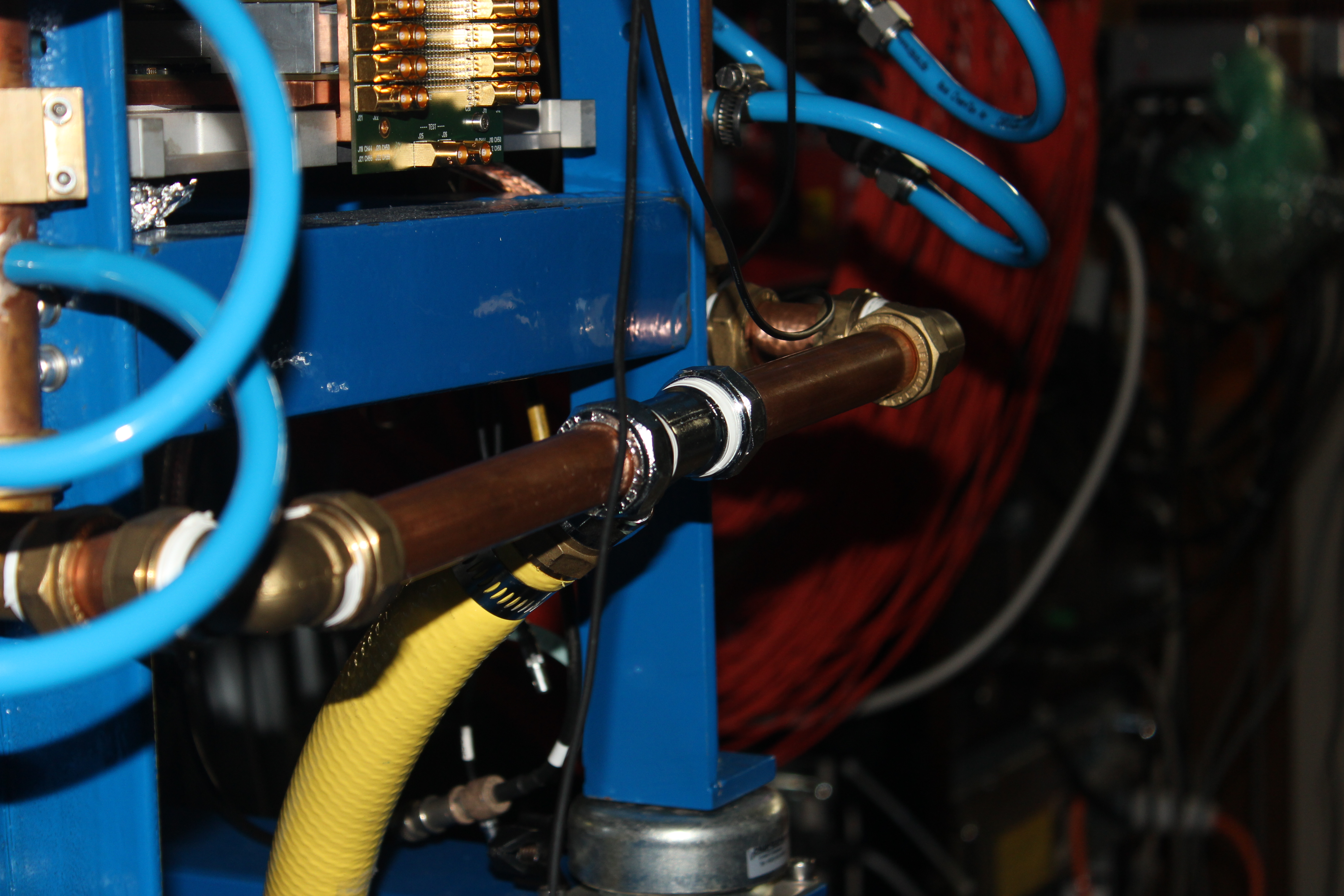
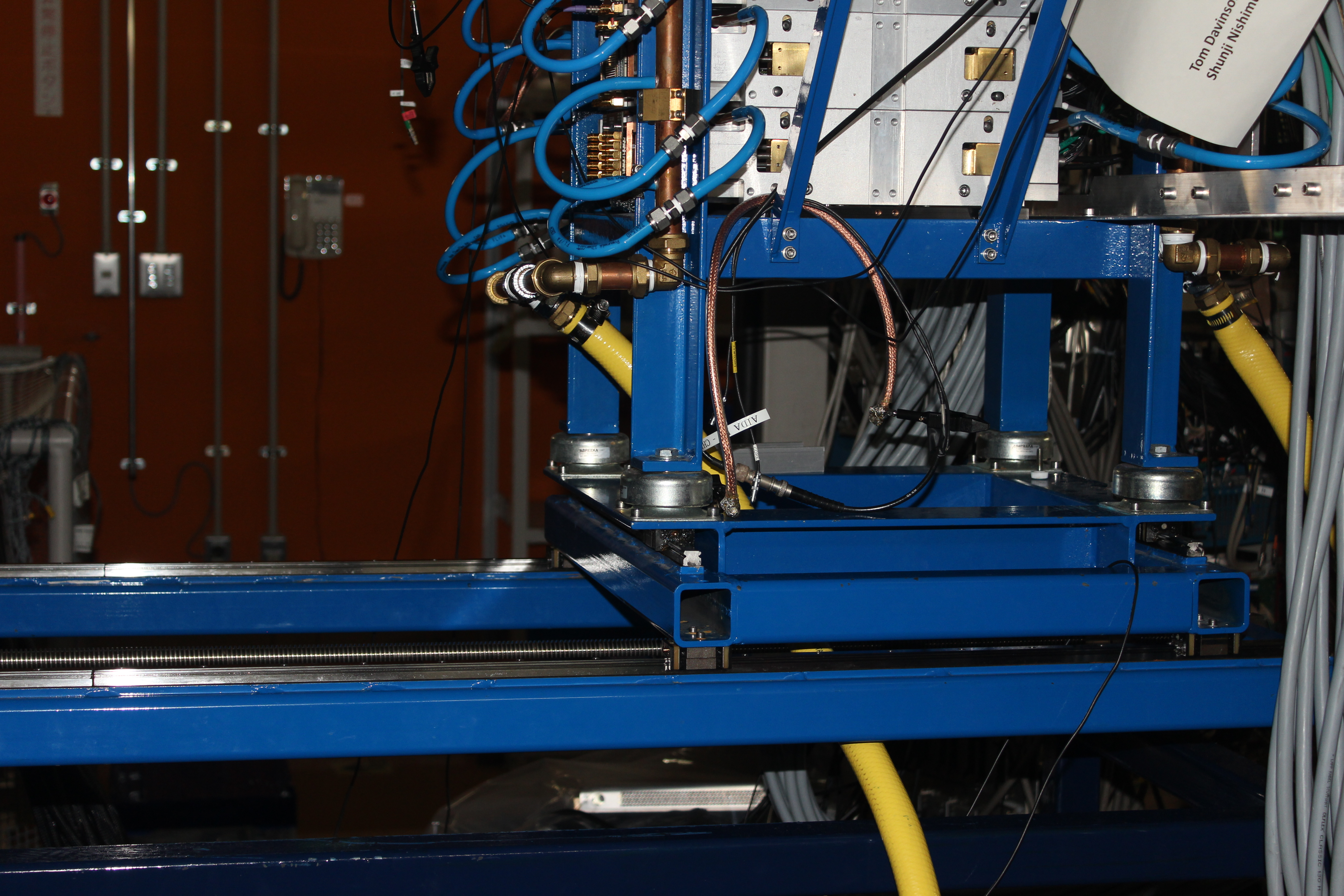
1130: Rotated forward water inlet connection to point towards rear of AIDA stand to remedy mechanical
      conflict with EURICA support frame - see attachments. During drain and re-fill of Julabo FL1106
      recirculating chiller no evidence of sediment in, or discoloration of, the water. Coolant loop closed
      and tested OK.

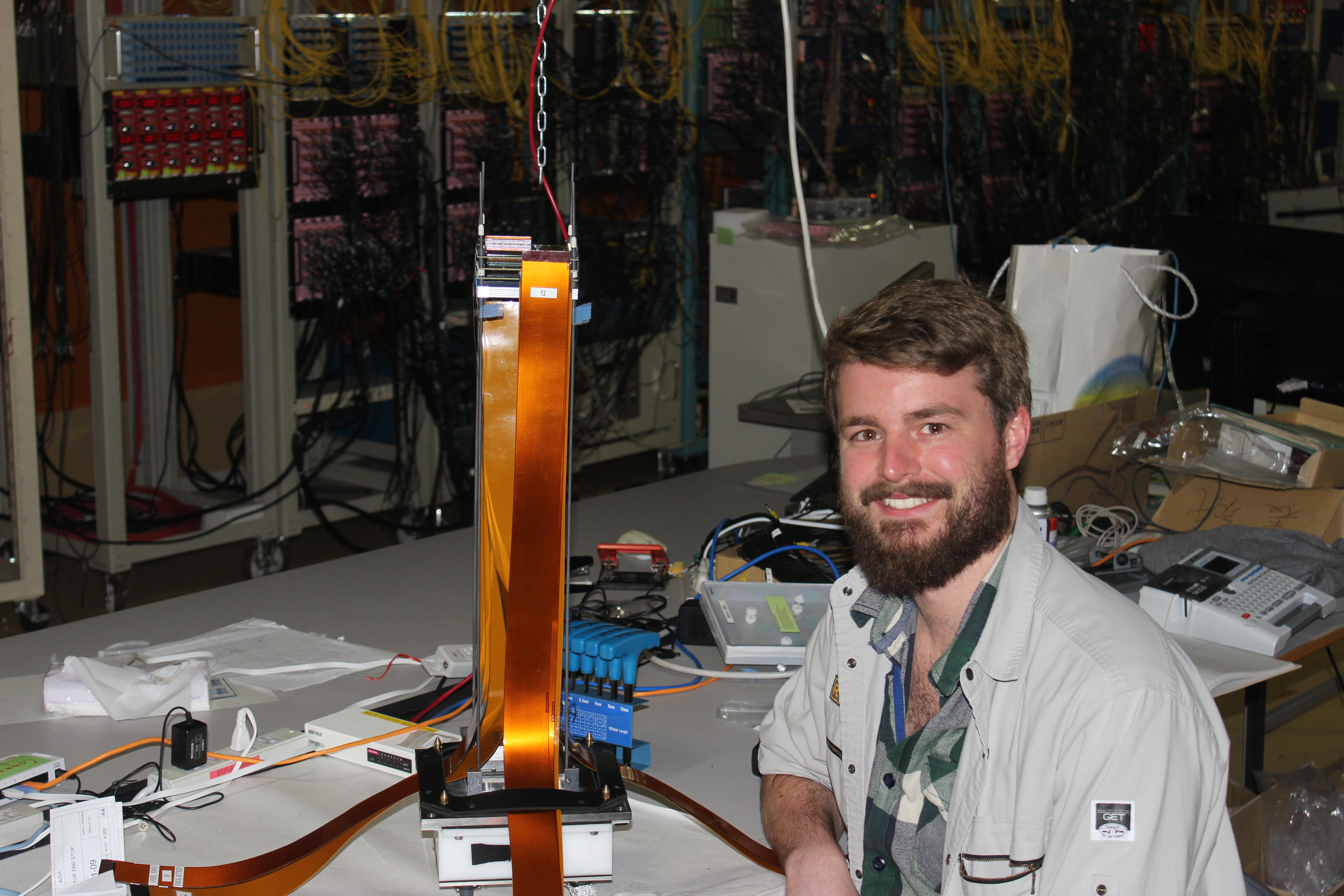
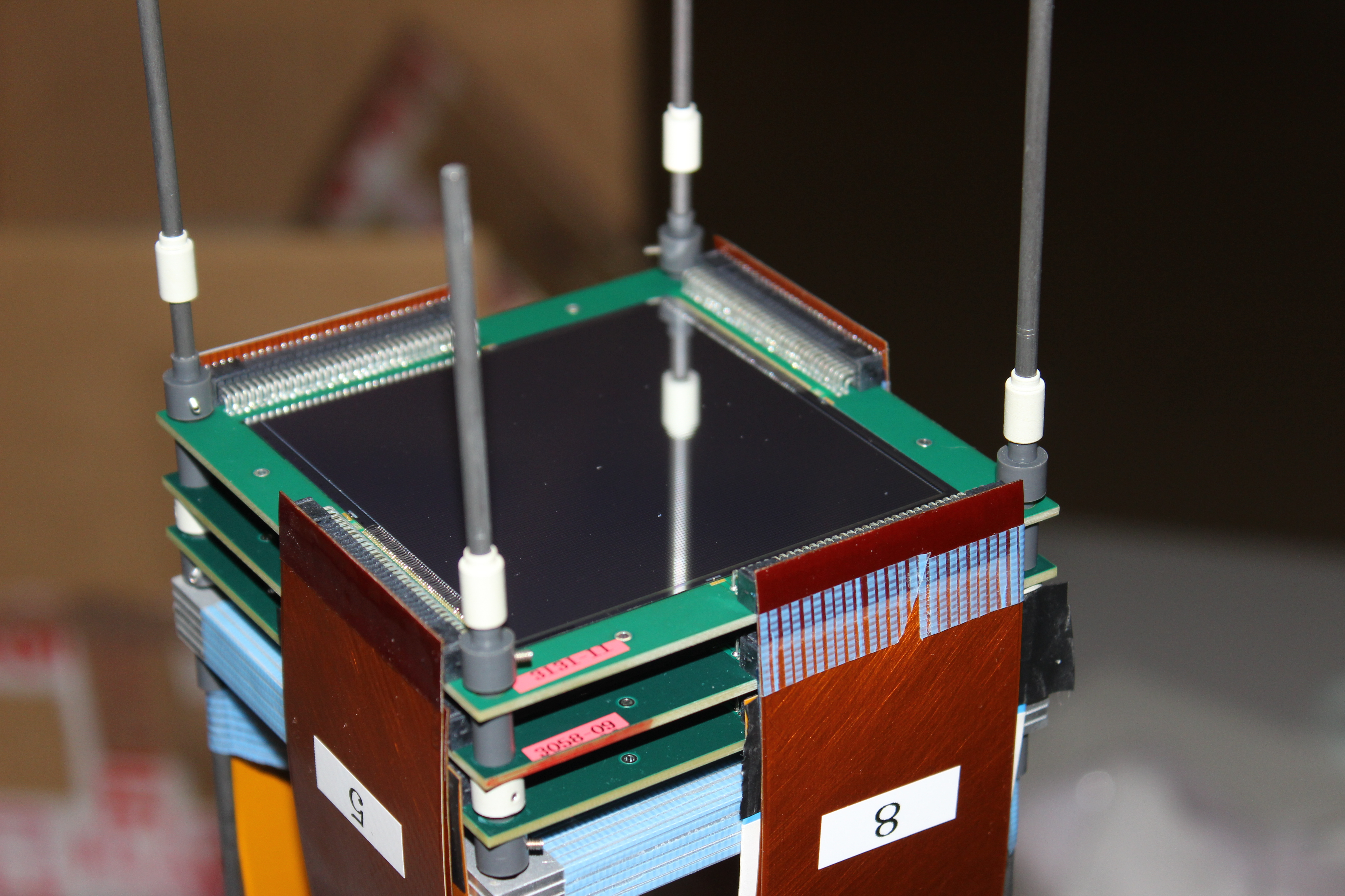
      CG installing (new, production batch) second and third MSL type BB18(DS)-1000 detectors to stack using
      the new FCT reduced capacitance 0.9m, 68-way to 68-way, flexible Kapton PCBs - see attachments.

1200: Installed two new BB18 detectors (3131-11 and 3058-09) to nose mount.
      Modified isolated kaptons labelled and number 1 and 5.
      Source (207Bi) mounted upstream of first detector approx 5-10mm away.

      Configuration - 3131-11 (#1) furthest upstream, 3058-09 (#2) in middle, 2977-20 (#3) at rear, followed by
10mm of Al.

1800: Cabled everything up.
      3131-11 connected to nnaida10+6 (p-side) and nnaida11+16 (n-side). HV from single supply.
      3058-09 connected to nnaida2+5 (p-side) and nnaida4+7 (n-side). HV from ch0 of quad supply.
      2977-20 connected to nnaida1+14 (p-side) and nnaida3+8 (n-side). HV from ch1 of quad supply.

      Typical resistance of new kaptons ~6.5 ohm.
      Typical resistance of old kaptons ~3.2 ohm.
      Makes sense if track width has been roughly halved, doubling resistivity.

      At +100V bias:
         - 3131-11 has leakage current 5.88 uA.
         - 3058-09 has leakage current 3.82 uA.
         - 2977-20 has leakage current 10.99 uA.

2000: Carried out brief pulser test of all connected modules.
      Many spectra exhibit double-peaking of the pulser peak or otherwise non-Gaussian peaks.
Of the ones the have single Gaussian shaped peaks, many now have much larger FWHM than previously observed. |
| Attachment 1: IMG_2852.JPG
|
|
| Attachment 2: IMG_2853.JPG
|
|
| Attachment 3: IMG_2858.JPG
|
|
| Attachment 4: IMG_2860.JPG
|
|
|
70
|
Fri Apr 24 08:11:04 2015 |
CG, AE & TD | Thursday 23 April 2015 contd |
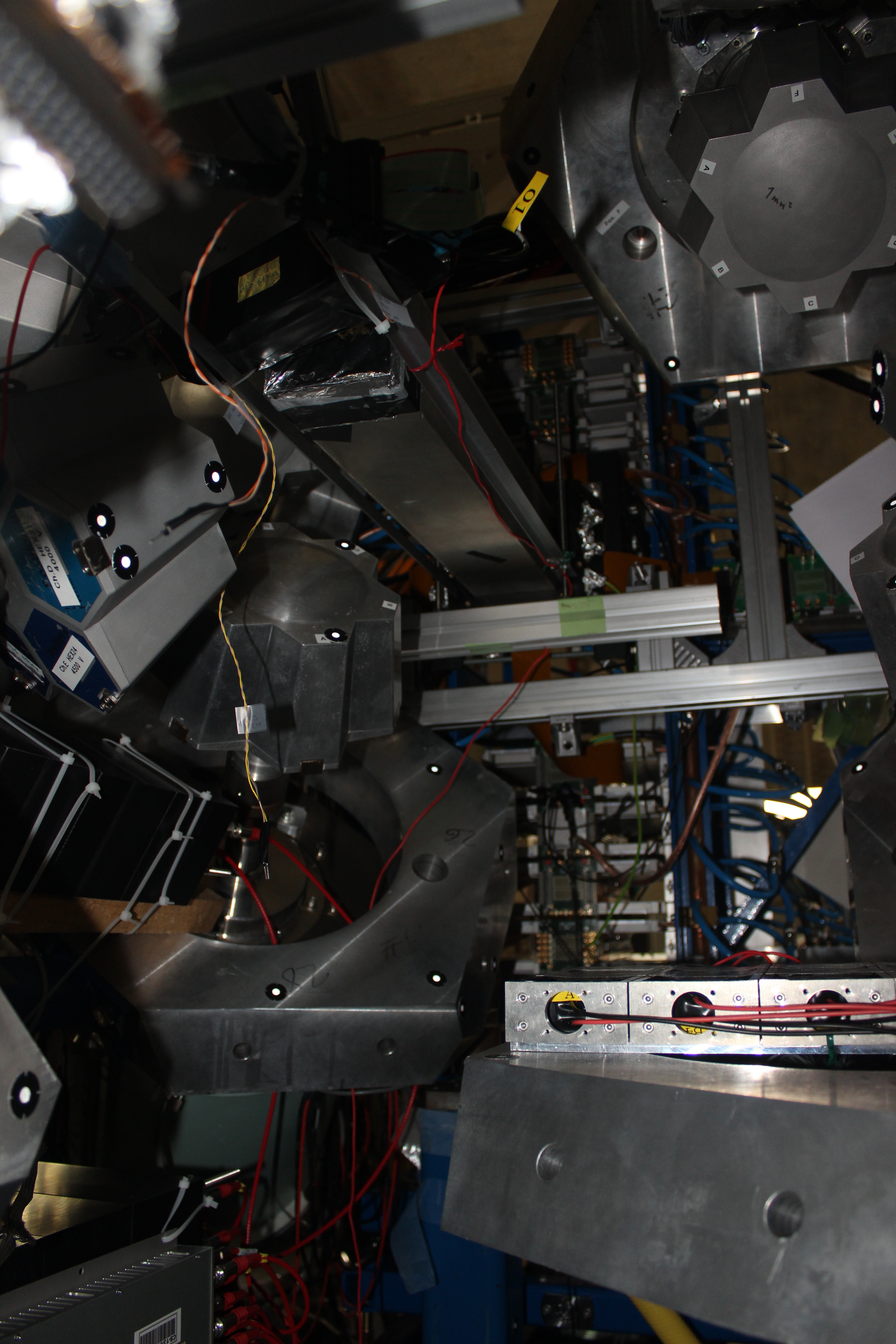
Image of interior of closed EURICA array with AIDA inserted. |
| Attachment 1: IMG_2850.JPG
|
|
|
69
|
Thu Apr 23 10:27:59 2015 |
CG, AE, TD | Thursday 23rd April progress |
23/04/15
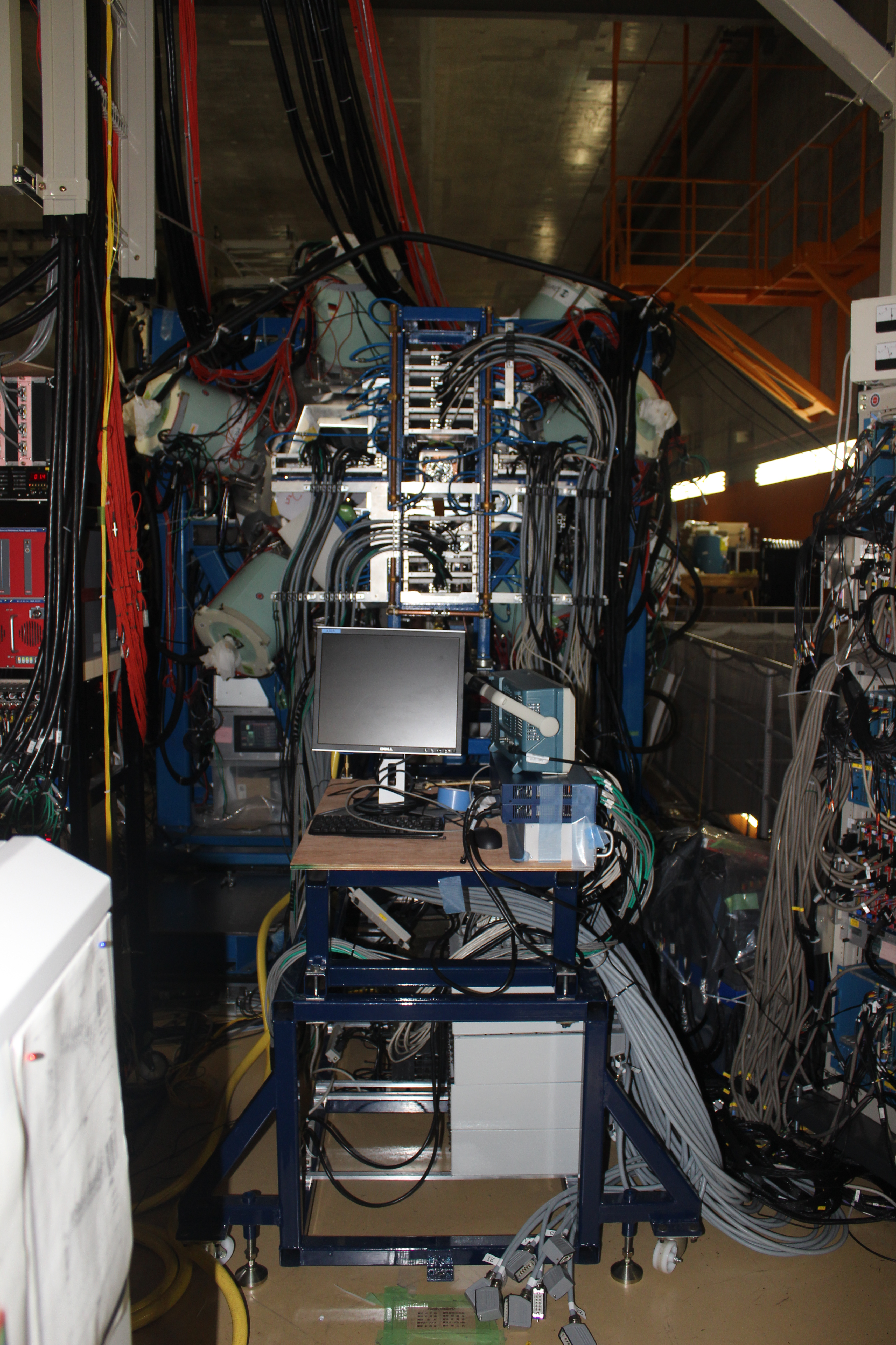
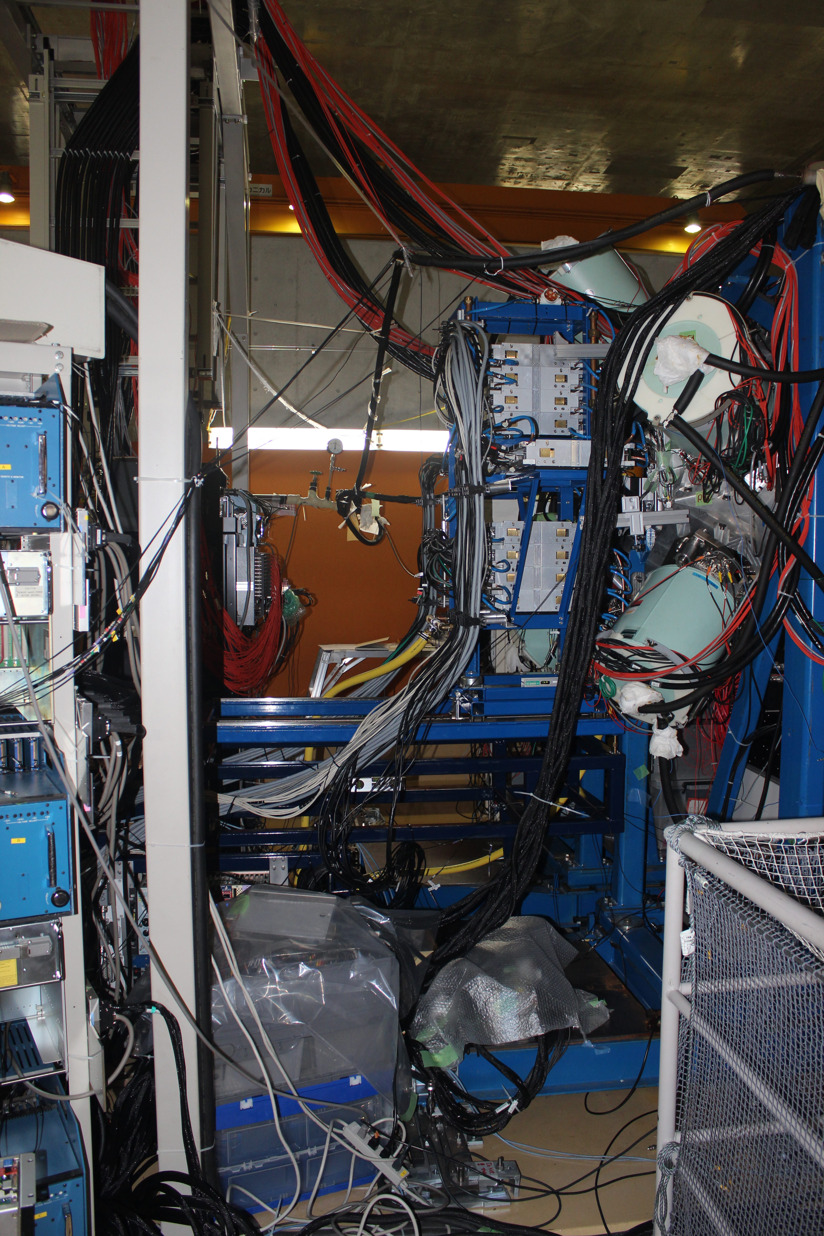
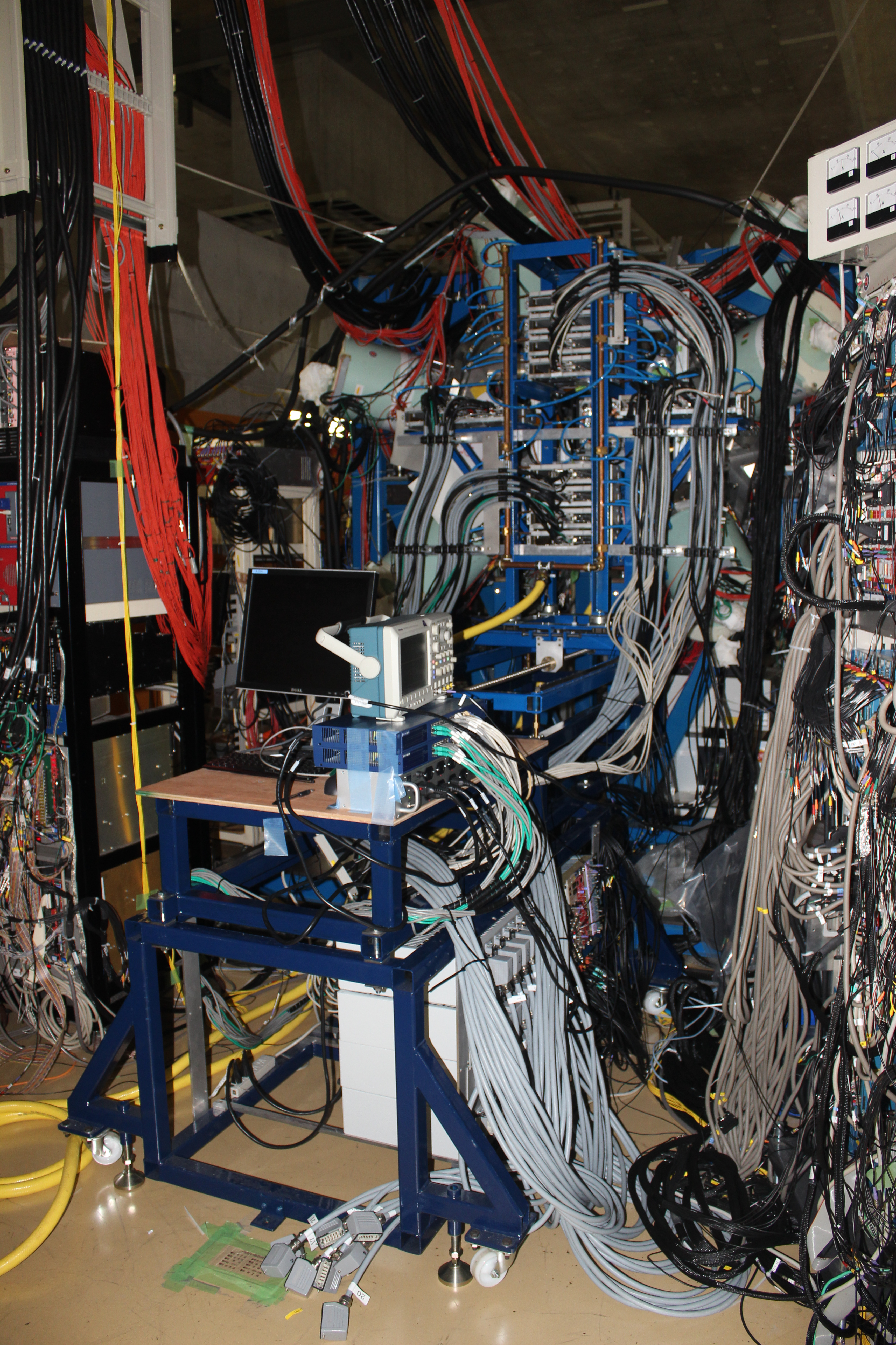
1800: Spent majority of the day moving AIDA forward and into EURICA.
So far everything seems to fit very well, we have just noticed a few points of possible mechanical conflict that should be watched when inserting/removing AIDA into EURICA
- Overhead LN2 pipes are lower than the top of the FEE tower. These have been loosely cable tied to some other cables to keep them away from AIDA. Need to make sure they don't move upon filling of LN2
- Yellow water pipe at front of AIDA may be pinched by EURICA structure upon full closure. Will check first time we close.
- Horizontal screw at base of nose is the most rearward point of contact and means AIDA cannot be inserted further than this. Already sufficiently far into EURICA so not a problem in that sense.
- Table itself can be moved to within ~5cm of EURICA structure without disturbing cabling along floor too much or touching rails.
- Front leg fits easily under EURICA structure.
Due to the number and file size of the photos, I can't upload them here so have made them available at:
https://www.dropbox.com/sh/ho1c0ocgc7rjji4/AADNsFZjSi6-Tx5CfxBt1PKUa?dl=0 |
| Attachment 1: IMG_2846.JPG
|
|
| Attachment 2: IMG_2847.JPG
|
|
| Attachment 3: IMG_2848.JPG
|
|
| Attachment 4: IMG_2849.JPG
|
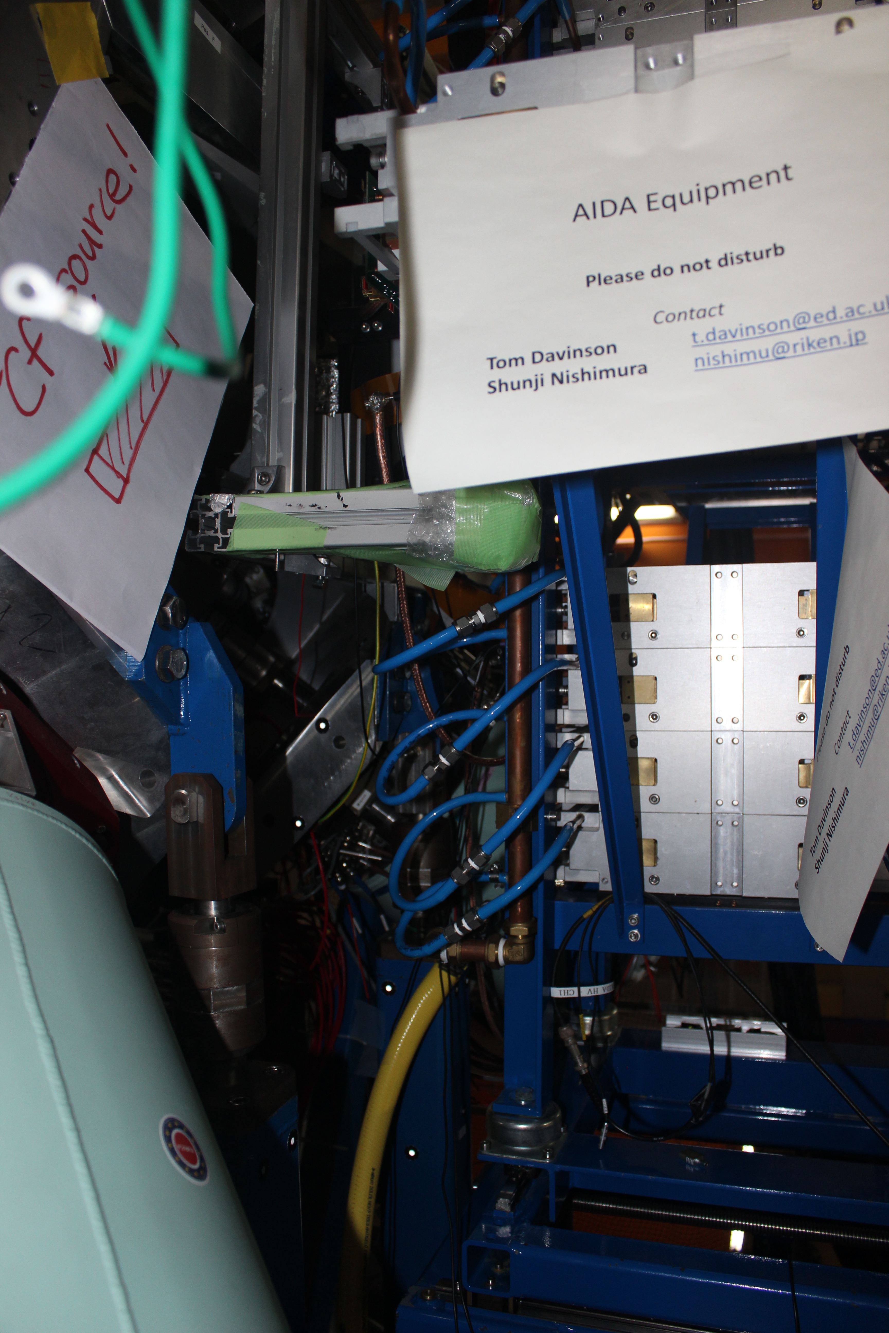
|
|
68
|
Thu Apr 23 09:02:57 2015 |
TD, Patrick | FEE64 Fast Discriminator OR o/p via MACB |
> Illustration of the trigger timing of the AIDA FEE64 fast discriminator OR output via the
> MACB front panel Trigger outputs.
>
> Channel 1: BNC PB-4 Pulser Trigger Output
> Channel 2: BNC PB-4 Pulser Analogue Output
> Channel 3: MACB Trigger Output
>
> MACB Trigger Output: NIM complement
>                      width ~ 7us
>                      delay ~ 750ns (with respect to BNC PB_4 Pulser Analogue Output)
>
> Example illustrates MAC Trigger Output from nnaida5 with standard ASIC settings and
> LEC/MEC fast discriminator 0x40

It would be useful to show the Trigger signal at the different levels of the MACB distribution system... then
the difference will show the delay through the MACB layer.

Are you able to estimate the length of cable between the pulser and the adaptor boards.

What are the conclusions about the delay .... is it too much to be useful ? |
|
67
|
Thu Apr 23 03:21:48 2015 |
TD | MSL type BB18(DS)-1000 |
MSL type BB18

Serial			Thickness	Depletion	Date		Note			Location
			(um)		(V)

2933-7			1004		?		7.11.11		Mechanical Sample	Edinburgh

2933-13/2933-18/2933-20	1001/1001/990	290/300/340	24.11.11	Mechanical Sample	Edinburgh

2944-4                  1034                                                                    RIKEN
2944-10                 1038                                                                    RIKEN
2944-15			1044									Edinburgh

2977-6			1004		75		6.6.12		Pre-production series   RIKEN
	bond wire repair reqd
2977-7			1010		70		26.7.12		Pre-production series   RIKEN
2977-15			1007		75		26.7.12		Pre-production series   RIKEN
2977-20			1008		70		6.6.12		Pre-production series   RIKEN


2998-20			1006		100		21.3.13					Edinburgh
2998-22			1006									Edinburgh
2998-23			1012									Edinburgh

3058-2			1016		60		17.11.14				Edinburgh
3058-3			1033		70		10.11.14				Edinburgh
3058-4			1023		60		7.11.14					Edinburgh
3058-5			1010		70		23.2.15					Edinburgh
3058-6			1013		66		12.11.14				Edinburgh
3058-7			1027		63		10.11.14				Edinburgh
3058-9			1029		60		11.11.14				RIKEN
3058-25			1011		115		3.3.15					RIKEN

3131-9			925		120		16.2.15					RIKEN
3131-11 923 80 6.3.15 RIKEN |
|
66
|
Wed Apr 22 08:50:59 2015 |
CG, AE, TD | Wednesday 22nd April progress |
22/04/15
1230: Solved problem (empty spectra despite changing modules) with nnaida5 noted in previous progress update.
During Feb tests, nnaida5 was very noisy compared to other nnaida => switched it to medium energy range to effectively turn it off.
This was saved in the default setting so this same configuration was loaded on startup.
Changed back to low energy mode, giving nnaida5 equally good performance as other nnaida, and altered system settings save file.
1630: Added heavy duty ground cabling to the copper blocks holding the adapter PCBs in loop around inner FEE modules with connections out to further out ones.
Removed PC-S copper braids with clippy ends.
Put electrical tape over the surrounding aluminium cooling crate to prevent electrical contact with that.
Using BB18 detector 2977-20 connected to FEEs 1, 3, 5, 8 using kaptons labelled E, B, F, G respectively.
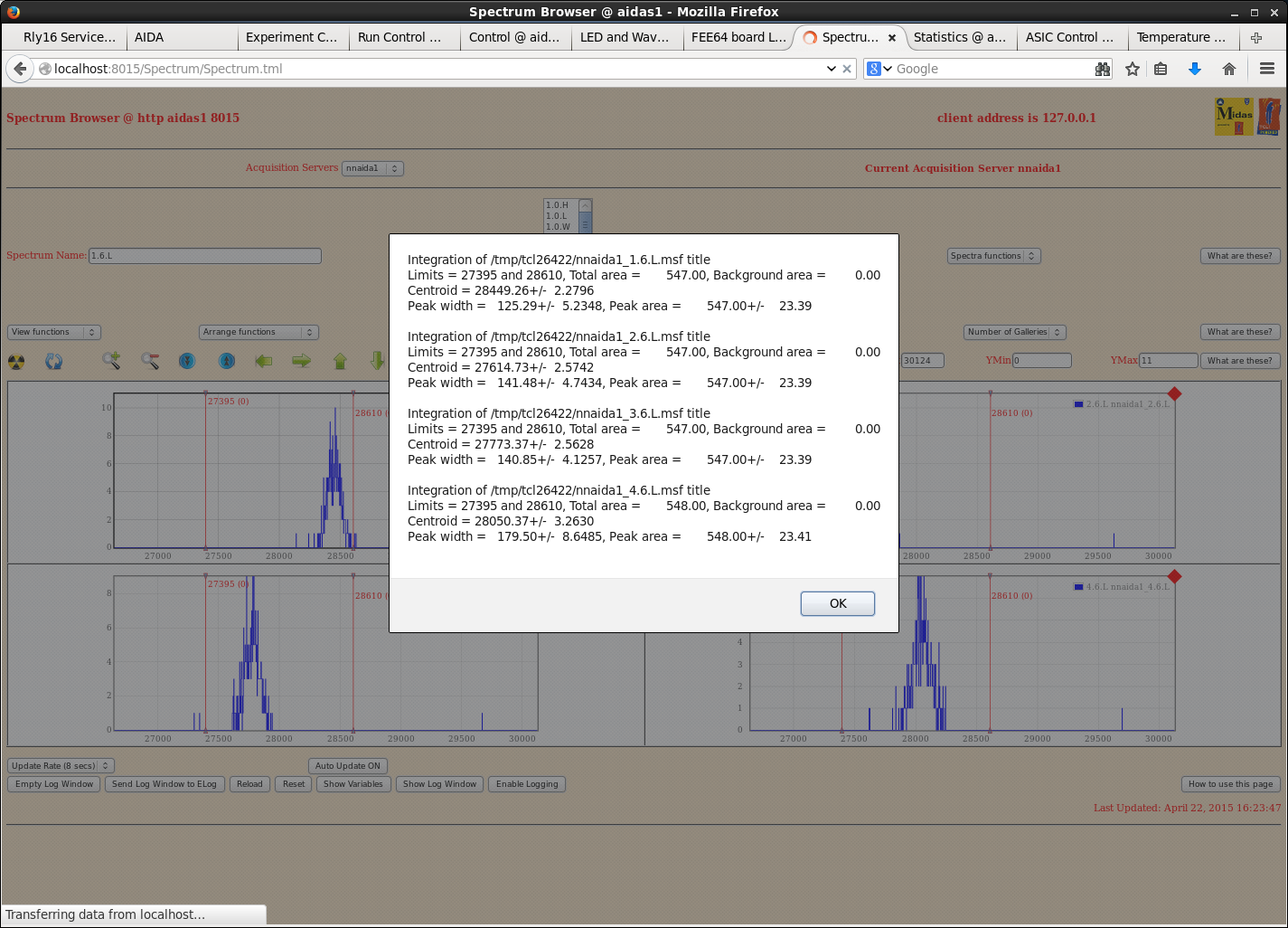
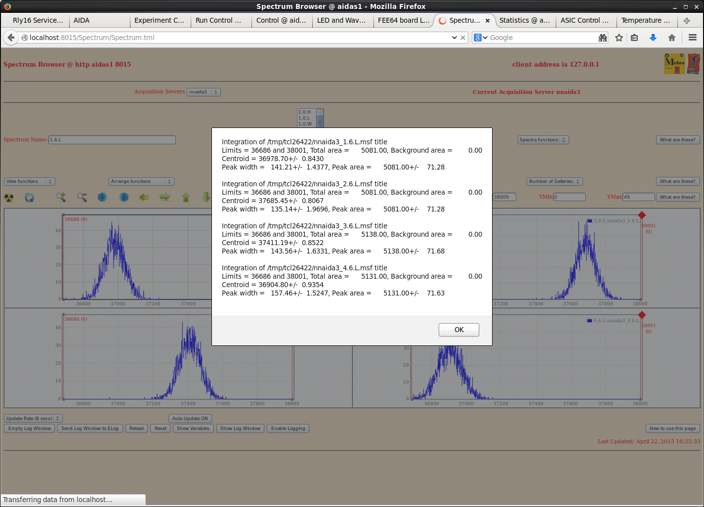
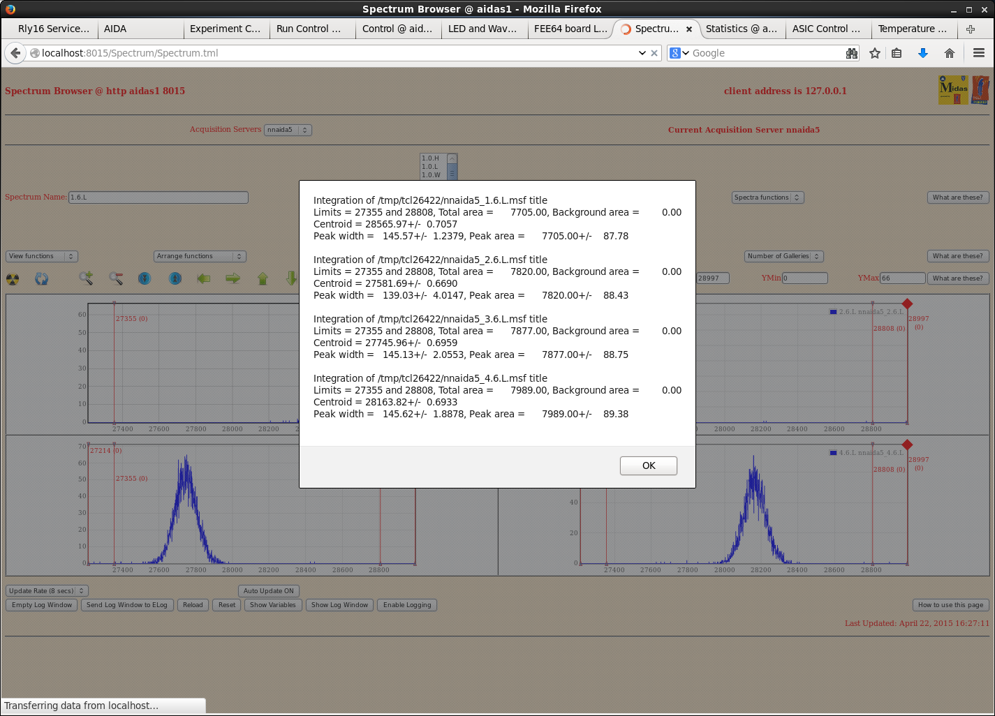
The FEEs connected to the detector saw much higher low-energy noise levels and typical FWHM of pulser peak increased by ~100ch to ~250ch.
Reduced shaping time and increased thresholds but saw no improvements.
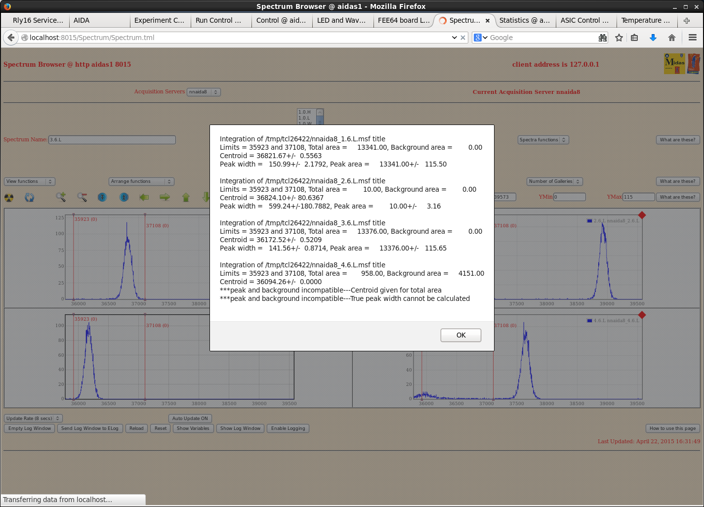
Refitted PC-S clippy copper braids in loop around inner most FEE modules and saw all pulser FWHM reduced to the ~130-150ch we saw during Feb tests (see attachments 1-4).
Suggests poor electrical connection between adapter PCBs and copper blocks.
1840: Added 4 new FEEs (nnaida25+26, 29+30) to system for use with new adapter PCBs accepting LEMO inputs from BigRIPS DAQ.
Edited /MIDAS/config/TclHttpd/aidas1@8015/startup.tcl to make system contain new FEEs.
Created new ASIC setting save file @ /MIDAS/DB/2015Apr22-extraInput.
nnaida25,29 have positive pre-amp polarity and nnaida26,30 have negative pre-amp polarity (along with other associated setting).
|
| Attachment 1: 20150422_nnaida1_FWHM.png
|
|
| Attachment 2: 20150422_nnaida3_FWHM.png
|
|
| Attachment 3: 20150422_nnaida5_FWHM.png
|
|
| Attachment 4: 20150422_nnaida8_FWHM.png
|
|
|
65
|
Wed Apr 22 07:28:25 2015 |
AE (PM) | Mechanical setup instructions: AIDA+EURICA at F11 |
Attached are Paul Morrall's instructions on how to move new AIDA support table into place, for a setup with
EURICA at F11 (March 2015). |
| Attachment 1: AIDA_procedure_document.docx
|
|
64
|
Wed Apr 22 03:33:01 2015 |
TD | FEE64 Fast Discriminator OR o/p via MACB |
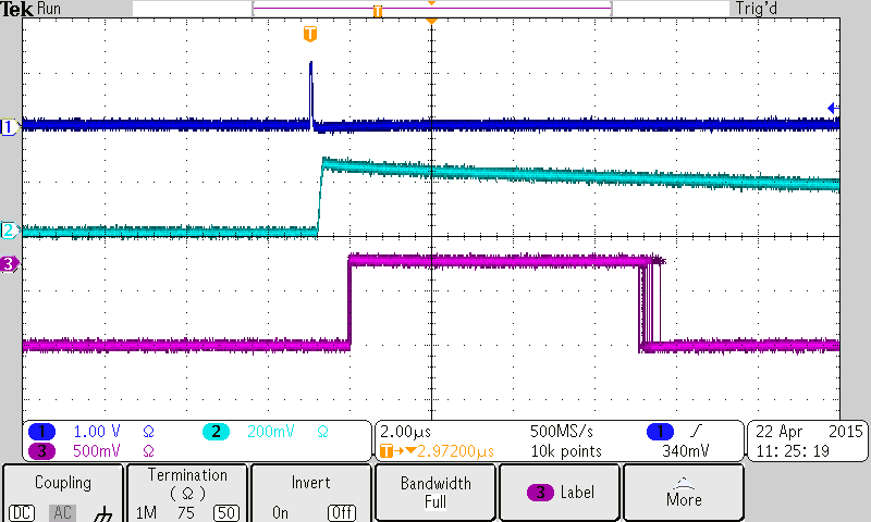
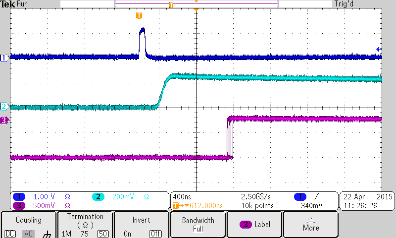
Illustration of the trigger timing of the AIDA FEE64 fast discriminator OR output via the
MACB front panel Trigger outputs.

Channel 1: BNC PB-4 Pulser Trigger Output
Channel 2: BNC PB-4 Pulser Analogue Output
Channel 3: MACB Trigger Output

MACB Trigger Output: NIM complement
                     width ~ 7us
                     delay ~ 750ns (with respect to BNC PB_4 Pulser Analogue Output)

Example illustrates MAC Trigger Output from nnaida5 with standard ASIC settings and
LEC/MEC fast discriminator 0x40 |
| Attachment 1: tek00000.tif
|
|
| Attachment 2: tek00001.tif
|
|
|
63
|
Tue Apr 21 09:39:00 2015 |
AE | LISE estimates for implantation setup [updated] |
[UPDATED 22/4: initial LISE file had incorrect thickness for MACi plastic]

Calculations for Al degrader thickness required to implant ions in AIDA DSSD stack.

Calculations are based on LISE files from main experiment, and done for settings with expected longest and shortest range
of
ions
before implantation setup:
- LISE++ for the 95Br BigRIPS setting : B1_U_BefissionZDSLAA_95Br_6mmF1.lpp
- LISE++ for the 85Ga BigRIPS setting : B1_U_BefissionZDSLAA_85Ga_6mmF1.lpp

Setup after last beamline detector (IC): 180cm Air + Al degrader + MACi (7mm plastic@45 degrees) + AIDA (3mm silicon) +
thick
Al
plate (1 cm).


+ 84Zn setting (long range):

 - Al degrader of 1 mm required in front of implantation setup to stop 84Zn activity in AIDA (end of stack).  The range in
Si
is
reduced by ~1.1 mm per each mm of Al added in degrader.

 - Activity from heavier (more intense) isotopes seems to be implanted at similar location as more exotic isotopes (always
considering 1p knockout channel, might be worth looking also at unreacted channels).

+ 94Se setting (short range):

 - Activity stopped before AIDA. We'll need to remove MACi if we want ions implanted in AIDA (unless the tail of energy
distribution
after secondary target is very large).

 - If we remove the MACi plastic, we would need 2 to 3 mm of Al degrader to stop ions in AIDA (assuming the 1mm veto after
segmented
MACi plastics remain).


See attachments for detailed description |
| Attachment 1: LISE_estimates_84Zn.docx
|
| Attachment 2: LISE_estimates_94Se.docx
|
|
62
|
Tue Apr 21 06:01:50 2015 |
CG, TD | Tuesday 21 April 2015 |
21/04/15
1325: Recabled the MACB distribution tree as per PC-S instruction yesterday.
Now have nnaida5+6, 13+14 in MACB3 (nnaida5 in output 1) and nnaida3+4, 11+12 in MACB10 (following the numbering system used in yesterday's ELog entry).
Complete system now happily resyncs on initial reset after power cycle.
nnaida7+15 still give a temperature reading of 0oC and nnaida8 is still running hot, but stable, at 65oC.
Visual inspection of cooling crate didn't reveal and air gaps between cooling plates and the FEE cards, or anything else to suggest there would be lower than expected cooling performance.
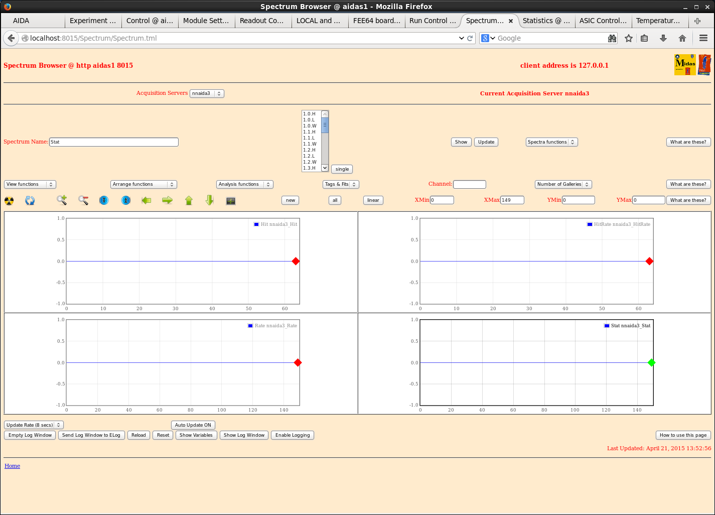
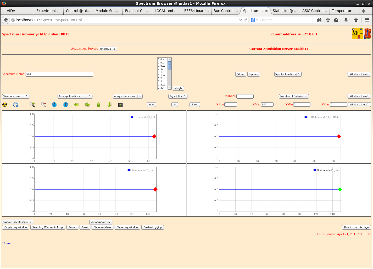
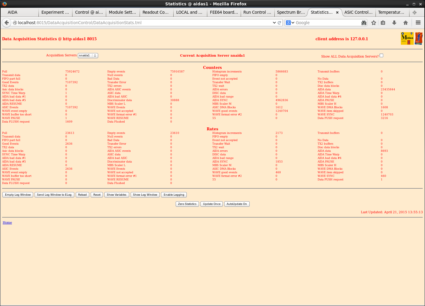
1340: After complete system start up, nnaida3+4, 11+12 now show absolutely no data (empty histograms, no good events/SYNC pulses in stats). (Attachments 1-4, example good spectrum/stats attachments 5-6)
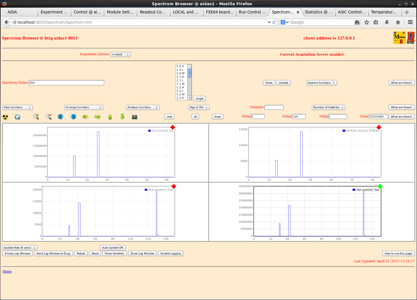
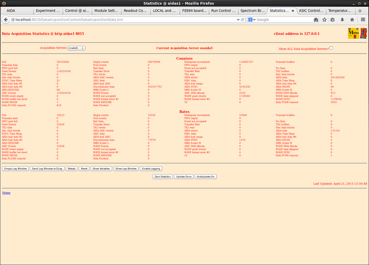
nnaida5 shows nonsensical data in histograms. (Attachments 7-8)
1500: Swapped HDMI cables from MACB NIM mdules cabling for FEE modules nnaida1+2, 9+10 for nnaida3+4, 11+12 - problem appears to move implying MACB is the problem
Swap MACB #13 for MACB #4 - problem resolved (still in position #10 as per CG numbering system used previously).
1600: nnaida5 does not produce sensible data - typically ~3-4 active channels with ADC and fast disc data with rates ~kHz/channel
Swap nnaida5 & 6 for (currently not used and not powered) nnaida27 & 28. Update /etc/dhcp/dhcpd.conf, restart dhcpd.
1800: Sync problem resolved, stable operation all afternoon including several system resets - no ReSync issues noticed. SYNC pulses provided to all FEEs consistently.
Connected detector BB18 2977-20 (same detector as used during Feb 2015 tests, with same kapton config as per 1520 on Feb 19th) to system with +ve 100V bias provided to n-side.
Updated firmware in new nnaida5+6 (formerly nnaida27+28) to be in line with all those currently in use.
Used saved ASIC settings from Feb 2015 visit and see similar FWHM in most spectra to those found during February after connecting heavy duty copper braids in loop between FEE modules in use.
nnaida5 still does not produce sensible data with almost identical spectra/stats to those seen before the module was replaced.
To be investigate tomorrow. |
| Attachment 1: 20150421_nnaida3_hitSpec.png
|
|
| Attachment 2: 20150421_nnaida3_stats.png
|

|
| Attachment 3: 20150421_nnaida11_hitSpec.png
|
|
| Attachment 4: 20150421_nnaida11_stats.png
|

|
| Attachment 5: 20150421_nnaida10_hitSpec.png
|

|
| Attachment 6: 20150421_nnaida1_stats.png
|
|
| Attachment 7: 20150421_nnaida5_hitSpec.png
|
|
| Attachment 8: 20150421_nnaida5_stats.png
|
|
|
61
|
Mon Apr 20 09:45:38 2015 |
CG, TD, Patrick Coleman-Smith | Progress 20th April + RPi procedure + reply ++ |
| Quote: |
|
| Quote: |
|
| Quote: |
|
20/04/15
1200: Complete all points on first part of check list, except checking the PSU voltages.
System now in powered and has all network/HDMI cables attached.
1300: Connect RPi to power switch but when powered on it didn't find the switch. A reliable procedure to start seems to be...
- connect USB power switch to RPI, make sure serial cable is disconnected from hub
- power up RPi and power switch
- check connection using dmesg, should see ...FT232RL for USB power switch on USB0
- check connection from aidas1 by pinging RPi inet address 10.1.1.251
- if good, Rly16 page should work from aidas1
- connect serial cable, open PuTTY session, select AIDA console settings, open
- should assign serial cable as USB1 an allow use of both the power switch and FEE console.
Currently this all works, we can control the power switch both from the RPi and aidas1, and see the FEE console via PuTTY session.
1400: Powered on system and tried to set up DAQ but received error (attachment 1) when doing the initial system reset in Run Control.
DAQ still usable for spectrum/temperature viewing, and all FEEs can be accessed to check ASIC control, but it seems timestamping will not be correct.
Tried to perform manual ReSync from master timestamp window and received similar error (attachment 2).
1430: nnaida8 running quite hot (ASIC temp ~65oC) and ASIC temp on nnaida7+15 read as 0.00oC. Otherwise, from pulser/stats data, both seem to be working correctly.
Unplugged power cable for nnaida7+8 at PSU end.
1600: Could timestamping issue originate from MACBs?
In rebuilding AIDA MACB - > FEE cabling redone. Should it follow a particular pattern/tree?
Current tree structure looks like (with MACB numbering going 1->11 L->R as you look at it):
MACB1 (setting: 0) ------- out 1: MACB2 (setting: 2) ---------- out 1: MACB3 (setting: 2) -> nnaida3+4, 11+12
&nb sp; &nb sp; ---------- out 2: MACB4 (setting: 3) -> nnaida19+20, 27+28
&nb sp; &nb sp; ---------- out 3: MACB5 (setting: 3) -> nniada1+2, 9+10
&nb sp; &nb sp; ---------- out 4: MACB6 (setting: 3) -> nnaida17+18, 25+26
&nb sp; --------- out 2: MACB7 (setting: 3) ---------- out 1: MACB8 (setting: 3) -> nnaida21+22, 29+30
&nb sp; &nb sp; ---------- out 2: MACB9 (setting: 3) -> nnaida7+8, 15+16
&nb sp; &nb sp; ---------- out 3: MACB10 (setting: 3) -> nnaida5+6, 13+14 -----> nnaida5 is the master and this comes from output2.
&nb sp; &nb sp; ---------- out 4: MACB11 (setting: 3) -> nnaida23+24, 31+32
Patrick - Is this set up OK? Do certain FEEs need to receive the MACB signal from certain MACBs or just all at the same point in the tree?
Also, MACBs 2+3 are on setting 2 on the dial, whereas the others (except MACB1, the 'grandparent') are set to 3. It seems like a hard thing to change accidentally so are they supposed to be like this or should they all be on the same setting?
1630: Voltages to nnaida7+8 OK at PSU output (+6V, +6V, +6V, -6.5V, +8V). Issue with contact to cooling rack?
With pulser input to all FEEs, only see pulser data in spectra for n-side (nnaida3+4, 7+8, 11+12, 15+16) FEEs. Other FEEs all show zero statistics.
|
The MACB system of clock and SYNC pulse distribution does have to follow some rules.
The Master needs to be in a very particular place. The rest are less important as long as they are all at the same level in the tree.
In the tree you report above and using the numbering you report. The Master should be in MACB3:out1.
The settings you have shown are correct if the Master is placed correctly ...
I will input a separate Elog entry detailing the settings for the MACB and the rules for the tree.
Thanks
Regarding nnaida7+8. I agree the issue to tackle first is the cooling plate contact to the module. Where do they feature in the layout ?
Is the plate tightened up correctly ?
As far as I am aware this module/crate has not recently been opened so the 'contact' should be as good (or bad) as it ever was.
But it would, of course, bear checking.
Regarding the P side FEE64s ... sorry about this ... but is the P pulser working ... well i did have to ask ;-
According to a DSO the positive and negative pulser inputs and cabling are OK
|
|
Regarding the P side problem.
What is the result if you change one of the N-Side FEEs to use the P-side pulser and vice-versa ?
Regarding the temperature problem.
Which position are the problem modules in ? |